
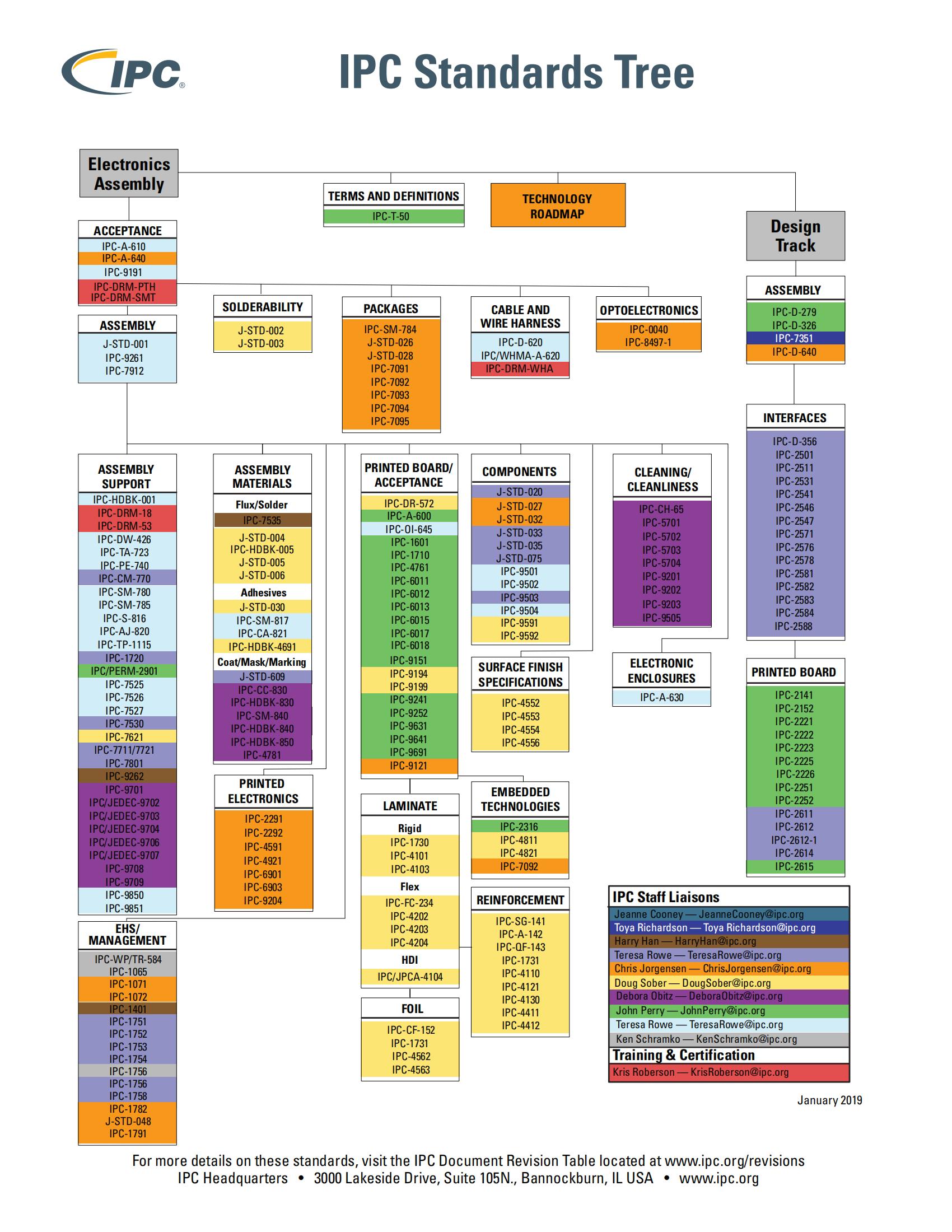
 NextPCB Capabilities
Printed Circuit Boards
NextPCB Capabilities
Printed Circuit Boards
 PCB Assembly
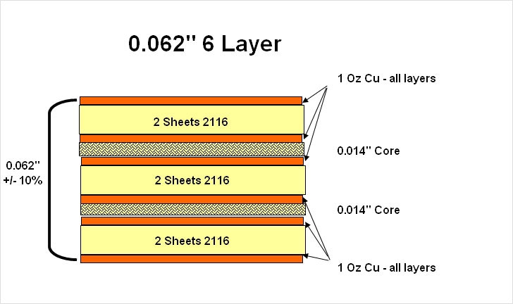
 Layer Buildup
 SMD-Stencils
 PCB Design-Aid & Layout
 Mechanics
 Quality
 Drills & Throughplating
 Factory & Certificate
 PCB Assembly Factory Show
Certificate
PCB Assembly Factory Show
Certificate
Support Team
Feedback:
support@nextpcb.com


IPC-2221 was originally published in 1998 by the Institute of Printed Circuits—now the Association Connecting Electronics Industries (IPC)—as a generic design standard for printed board assemblies. The B revision followed in November 2012, tightening several numerical constraints and expanding coverage of high-density interconnect (HDI) topologies. IPC-2221C, released in December 2023, is the current governing revision and supersedes IPC-2221B in its entirety.
The C revision is not a cosmetic update. It introduces substantive new sections covering back-drilling, compliant pins (press-fit), plated board edges, palletization as distinct from panelization, formal impedance tolerance tables, clearance areas in planes, and updated feature location tolerances. It also substantially revises the minimum electrical clearance guidance—particularly the altitude-dependent conductor spacing requirements that IPC-2221B handled less precisely—and formalizes the Comparative Tracking Index (CTI) material classification that was previously referenced by implication. Most EDA tool templates and online trace-width calculators in active use as of 2026 still reference IPC-2221B tables; designers working against customer specifications that cite "IPC-2221" should verify which revision is intended.
The standard does not dictate one specific design outcome. It establishes minimum acceptable thresholds for dimensions, spacing, and material properties, leaving room for product-specific requirements to exceed those thresholds. In practice, most contract manufacturers have their own internal capability documents that sit alongside IPC-2221C—typically tighter in some areas (e.g., minimum annular ring on blind vias), looser in others (e.g., board edge clearance for panelized V-score). Understanding where your fabricator diverges from the base standard is more actionable than treating IPC-2221C as an absolute rulebook.
IPC-2221C is the foundation document for the IPC-2220 series. The sectional standards—IPC-2222 (rigid organic PCBs), IPC-2223 (flexible circuits), IPC-2226 (HDI), and IPC-2228 (semiconductor packaging substrates, now explicitly listed in 2221C)—supplement rather than override the base standard. For rigid-flex, IPC-2221C and IPC-2223 apply simultaneously; the more restrictive requirement governs. Where IPC-2221C does not cover a technology, designers typically reference IPC-6012F (qualification and performance, current revision) or IPC-7711/7721 (rework) as supplementary documents.
IPC-2221C updated the material and copper foil selection guidance relative to IPC-2221B, formalizing several criteria that the earlier revision addressed only implicitly. The engineering judgment still happens in the gap between what the standard permits and what a given design actually needs.
Standard fabrication defaults to 1 oz/ft² (35 μm) copper on outer layers and 0.5 oz/ft² on inner layers. IPC-2221C does not mandate these values; it defines minimum thickness requirements relative to current-carrying capacity requirements. A distinction added more clearly in the C revision is between electrodeposited (ED) and rolled-annealed (RA) copper foil: RA copper has better elongation-to-failure properties, which matters in flex regions and high-cycle thermal applications, while ED is the standard for rigid boards. The choice affects both the fabrication process and the reliability model under thermal cycling.
IPC-2221C explicitly defers current-carrying capacity calculations to IPC-2152 rather than relying on the legacy empirical curves from earlier revisions. The IPC-2221 Annex B and C charts—derived from 1950s experimental data—remain reproduced in the standard as reference, but IPC-2152 provides a more accurate dataset that accounts for copper pour geometry, adjacent copper density, and thermal boundary conditions. For power designs, using an IPC-2152-based calculator rather than one labeled "IPC-2221" is the more defensible choice. Moving to heavy copper (4 oz and above) puts a design outside standard process capability at many fabs regardless of what either standard permits on paper, requiring explicit DFM discussion before committing to a stack-up.
FR-4 covers the majority of consumer and industrial applications. The relevant parameter from an IPC-2221C standpoint is Tg (glass transition temperature)—standard FR-4 has a Tg around 130°C, while mid-Tg grades run 150–170°C, and high-Tg (180+) materials are used in automotive and high-reliability assemblies. The C revision adds formal treatment of Comparative Tracking Index (CTI) through Table 6-2, which classifies substrate materials into groups based on their resistance to surface tracking under high voltage. CTI was referenced implicitly in IPC-2221B; in IPC-2221C, the material group classification from Table 6-2 feeds directly into the conductor spacing requirements for creepage in Table 6-1. This connection between material selection and spacing requirements is more explicit in the C revision and cannot be ignored in safety-critical or high-voltage designs.
For RF and high-speed digital applications, the material choice shifts to controlling dielectric constant (Dk) and dissipation factor (Df). PTFE-based laminates (Rogers RO4000-series, Taconic) offer Dk values around 3.2–3.5 with Df below 0.004 at 10 GHz. FR-4 Dk varies from 4.2 to 4.8 depending on resin content and frequency, which introduces trace-length-dependent timing errors at multi-GHz signaling rates. IPC-2221C does not specify Dk tolerances directly; that falls to IPC-4101 and the laminate manufacturer's datasheet.
IPC-2221C also formally addresses Conductive Anodic Filament (CAF) growth in Section 6.3.4. CAF is an electrochemical failure mechanism where copper migrates through the glass fiber/resin interface under DC bias, creating a conductive path between adjacent conductors or vias. It is most pronounced in high-humidity environments with tight via spacing and high voltage differentials. The C revision's inclusion of CAF as an explicit design consideration—rather than a manufacturing quality issue alone—reflects industry experience with failures in dense board designs where spacing met IPC-2221B minimums but CAF was not assessed. Laminate selection with low CAF susceptibility (measured per IPC TM-650 Method 2.6.25) is relevant in telecommunications, automotive, and server applications with long field life requirements.
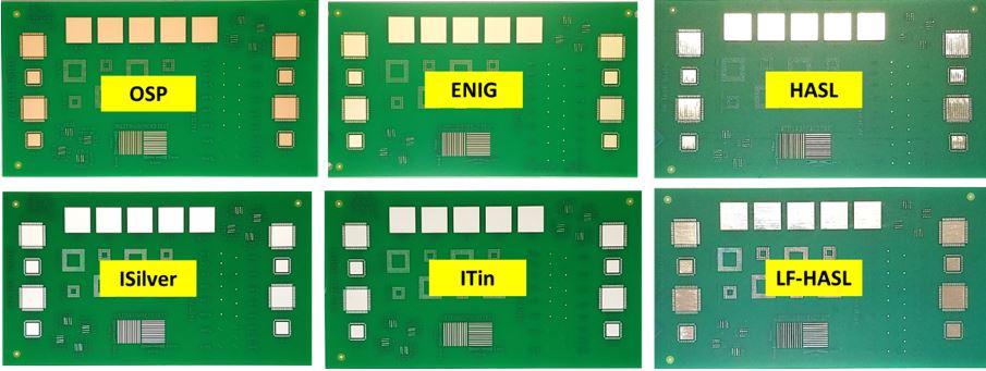
The tradeoff between surface finishes is well-understood, but the IPC-2221C-relevant consideration is shelf life and solderability. HASL (hot air solder leveling) remains the lowest-cost option but produces uneven pad surfaces that create coplanarity issues with fine-pitch QFPs and BGAs. ENIG (electroless nickel immersion gold) provides flat, consistent surfaces at higher cost; the risk is "black pad" failure if the nickel layer is improperly controlled. OSP (organic solderability preservative) is RoHS-compliant and low cost, but degrades with multiple thermal cycles and requires careful handling between fabrication and assembly. Immersion silver offers good RF performance but tarnishes in storage. Hard gold is reserved for edge connectors and contact surfaces where wear resistance is needed, including castellated edge connector fingers covered under the C revision's expanded edge plating guidance.
IPC-2221C references surface finish requirements in the context of solderability and minimum pad geometry. For specific finish thickness requirements, IPC-4552 (ENIG), IPC-4553 (immersion silver), and IPC-4554 (immersion tin) are the governing documents.
IPC-2221C restructured the board size and manufacturing section relative to IPC-2221B, most notably by separating panelization (Section 5.6) from palletization (Section 5.7) as distinct processes, and by adding Section 5.8 on plated board edges. These additions reflect manufacturing realities that were not formally addressed in the B revision.
Aspect ratio in IPC-2221C terminology refers to the ratio of board thickness to minimum drilled hole diameter. A 1.6 mm board with 0.3 mm drill diameter has an aspect ratio of approximately 5.3:1. Most standard fabs handle 8:1 to 10:1 without issue. Beyond 12:1, copper plating uniformity inside the barrel degrades, introducing risk of opens or voids in the via wall. HDI designs with laser-drilled microvias (typically 0.075–0.125 mm diameter) sidestep this constraint by using sequential lamination rather than through-hole drilling.
IPC-2221C maintains the minimum copper-to-board-edge clearance guidance from the B revision (0.25 mm for routed edges as a working minimum). For V-scored panels, where the actual break line can shift due to scoring depth tolerance, 0.5 mm is a safer working value. Sharp internal corners in routed cutouts remain a stress concentration point; the minimum router bit diameter for standard tooling (typically 0.8 mm) limits achievable internal corner radii, and ignoring this causes dimensional tolerance issues in production.
IPC-2221C distinguishes explicitly between panelization and palletization for the first time. Panelization refers to assembling multiple PCBs into a single fabrication array—the familiar V-score or tab-routed panel used in SMT assembly. Palletization, addressed in new Section 5.7, refers to the use of a carrier fixture or pallet to hold individual boards or assemblies during processing, particularly for non-standard form factors. The datum feature requirements in Section 5.4.3.1 were updated specifically to support palletization setups, which require unambiguous fiducial placement for automated equipment registration. If a design uses palletization at the CM, the IPC-2221C datum requirements are the design-level starting point for the pallet fixture design conversation.
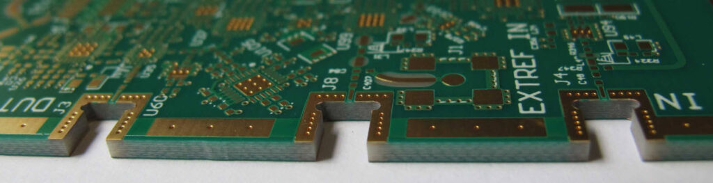
Section 5.8 on plated edges is new in IPC-2221C and does not have a direct equivalent in IPC-2221B. It addresses perimeter edge plating—where copper is plated on the board edge itself rather than only on pads and traces. This is relevant for edge-launch RF connectors, EMI shielding applications, and thermal management designs where the board edge connects to a chassis ground. The section specifies the minimum edge plating coverage requirements and the associated routing and drilling constraints. Designs that previously had to negotiate edge plating requirements informally with the fab now have a standard reference to cite. Note that edge plating adds process steps and is not part of standard fab quoting; it must be called out explicitly in the fab notes and typically carries a surcharge.
Mounting holes are mechanical attachment points, but their placement affects board stress during assembly and in-service vibration. IPC-2221C requires a copper-free keepout around plated mounting holes unless they are intentionally connected to a ground plane. For compliant pin (press-fit) hardware—now covered in their own section in IPC-2221C—the hole diameter tolerance, PCB material compressibility, and pin insertion force interact in ways that require explicit validation. See the Compliant Pin section below.
Component placement in IPC-2221C is addressed from the standpoints of electrical path length, manufacturability, and thermal behavior. The standard does not define optimal placement—it defines minimum clearances and orientation constraints that prevent failures. The C revision's updated feature location tolerances (Section 5.4.2) are relevant when tight component placement relative to board features is a design requirement.
The minimum component-to-component clearance depends on the assembly process. For hand soldering or selective soldering, 0.5 mm between component bodies is workable. For automated SMT reflow with no secondary operations, 0.2 mm is achievable if the stencil design accounts for solder-bridging risk. Wave soldering adds constraints for components on the bottom side—tall components shadow adjacent pads from the solder wave, creating solder skips. IPC-2221C does not define all these scenarios precisely; IPC-7525 (stencil design) and IPC-7711/7721 (rework) carry some of this burden. EDA courtyard layers and IPC-7351 land pattern standards are the working reference for placement clearance, with IPC-2221C as the governing background document when disputes arise about whether a layout meets minimum acceptable standards.
Polarized components (electrolytic capacitors, diodes, ICs) have orientation requirements driven by electrical correctness, not IPC-2221C. Where the standard is relevant is in specifying that component orientation should minimize electrical path length for high-frequency signals and allow consistent visual inspection after assembly. For reference designator legibility and automated optical inspection (AOI), IPC-A-610 is the more directly applicable acceptance document.
IPC-2221C guidance on thermal component placement addresses two separate problems: preventing heat-sensitive components from being adjacent to heat-generating ones, and ensuring that high-power components have adequate thermal dissipation paths. Keeping temperature-sensitive components (voltage references, crystal oscillators, precision resistors) away from power conversion circuitry is straightforward in principle but requires thermal simulation to validate in dense designs. For power semiconductors, the standard references thermal resistance in terms of the PCB's ability to spread heat; placing a high-dissipation component at the board center maximizes spreading resistance if the board is a simple FR-4 stack, while moving it near an edge with exposed copper pours reduces the thermal path to ambient.
The conductor sizing and spacing requirements in IPC-2221C carry forward the structure of IPC-2221B but with notable updates: a more explicit referral to IPC-2152 for current-carrying capacity, revised altitude-dependent spacing in Table 6-1, and a new formal impedance tolerance table (Table 6-4) in Section 6.4.
IPC-2221C retains the empirical Annex B and Annex C charts for internal and external conductors respectively, but the accompanying text more explicitly acknowledges that IPC-2152 is the preferred reference for current-carrying capacity calculations. The legacy formula underlying the Annex charts is:
I = k × ΔT0.44 × A0.725
Where I is current in amperes, ΔT is the allowed temperature rise in °C, A is the cross-sectional area in mil², and k is 0.048 for internal layers, 0.024 for external layers. This dataset originates from 1950s experimental work and does not accurately model modern conductor geometries—particularly wide copper pours, embedded copper planes, or traces with heavy copper adjacent to ground pours. For any design where conductor temperature is a performance or reliability constraint, IPC-2152 is the more defensible calculation basis. Most online calculators labeled "IPC-2221" use the legacy k-values; most labeled "IPC-2152" use the updated dataset.
Minimum conductor spacing in IPC-2221C is a function of voltage differential between adjacent conductors and the operating environment. Table 6-1 in the standard provides the minimum spacing matrix across conductor types (internal, external coated, external uncoated) and voltage ranges. For sea-level uncoated external conductors at voltages up to 30 V DC, the minimum spacing remains 0.1 mm—consistent with IPC-2221B. The material change in IPC-2221C is in the high-altitude and vacuum conductor categories.
IPC-2221C expanded the altitude-dependent spacing requirements, adding explicit treatment for designs operating above 3050 m (10,007 feet) or in vacuum environments. At altitude, reduced air density lowers dielectric strength, requiring larger conductor separations for the same working voltage. The A8 conductor category—external leads without conformal coating above 3050 m or in vacuum—carries substantially higher spacing requirements than the equivalent sea-level uncoated case. This distinction matters for aerospace, high-altitude drone, and satellite applications. IPC-2221B addressed altitude only loosely; the C revision provides more specific guidance that aligns better with IEC 62368-1 and other safety standards that electronics manufacturers targeting these markets must comply with.
The CTI material group from Table 6-2 also feeds into Table 6-1 for creepage distance calculations in high-voltage designs. A substrate with a lower CTI group requires larger creepage spacing for the same working voltage. This was an implicit relationship in IPC-2221B; IPC-2221C makes it explicit and traceable.
IPC-2221C added guidance on clearance areas within copper planes—the anti-pad geometry around drilled holes and vias that pass through a plane layer without making electrical contact. This was underspecified in IPC-2221B, which led to inconsistent anti-pad sizing between designs and occasional impedance discontinuities in high-speed designs where the anti-pad diameter controls the local impedance environment of the via. The C revision provides a framework for sizing anti-pads relative to the via drill and annular ring requirements, reducing reliance on arbitrary fab defaults.
One of the more practically useful additions in IPC-2221C is Section 6.4 on impedance controls, which includes Table 6-4 providing example impedance tolerance targets. IPC-2221B acknowledged impedance control as a design requirement but provided no quantitative tolerance framework within the standard itself. IPC-2221C formalizes what the industry had been specifying informally: typical production tolerance for controlled impedance is ±10% on target values, achievable on standard fabrication lines with dielectric height control and etch compensation. Tighter tolerances (±5%) are achievable but require tighter laminate thickness control, etching process control, and typically a test coupon acceptance requirement on every panel.
The practical implication is that fabrication drawings citing IPC-2221C can now reference Section 6.4 and Table 6-4 when specifying impedance requirements, rather than defining all tolerance criteria in custom fab notes. This does not eliminate the need for explicit impedance specifications on the drawing, but it provides a shared baseline that reduces ambiguity in procurement and supplier qualification.
Differential pairs (USB, PCIe, LVDS, Ethernet) have constraints beyond single-ended traces. IPC-2221C addresses the need for consistent intra-pair spacing to maintain impedance matching and minimize common-mode noise conversion. In practice, this means keeping the intra-pair gap constant, minimizing length mismatch within the pair, and routing both members with equal-length bends (not 90° corners, which generate reflections at frequencies above approximately 1 GHz). The standard provides the framework; signal integrity simulation and post-layout extraction are the validation tools.
Via design in IPC-2221C covers the mechanical and electrical requirements for through-hole connections between PCB layers. The C revision adds a formal section on back-drilling that was absent from IPC-2221B, alongside the via type, sizing, and plating guidance carried forward from earlier revisions.
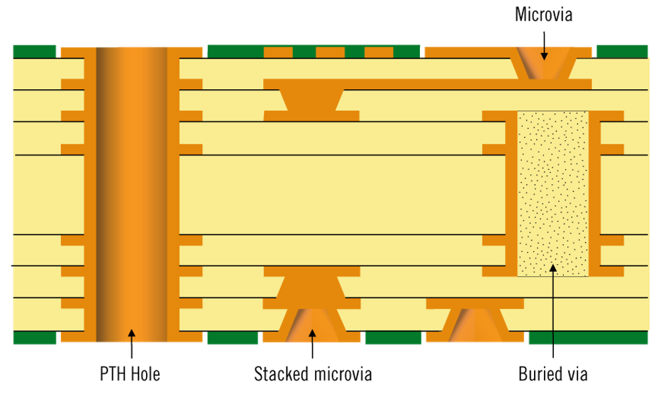
Through-hole vias penetrate the full board stack and are plated in a single electroplating operation—lowest cost and highest baseline reliability. Blind vias connect an outer layer to one or more inner layers without penetrating to the opposite side; they require depth-controlled drilling, which adds process complexity and cost. Buried vias exist entirely within the inner layers and require sequential lamination, adding two to four additional lamination cycles and proportionally increasing cost and lead time. Microvias (laser-drilled, typically 0.075–0.125 mm diameter) are used in HDI designs to achieve pad density that mechanical drilling cannot reach. IPC-2221C covers the base requirements for all types; IPC-2226 (HDI design standard) provides more detailed guidance on microvia stack configurations and their reliability implications.
Back-drilling is now formally addressed in IPC-2221C as a via optimization technique for high-speed digital designs. In through-hole vias used in multilayer boards, the portion of the via barrel that does not connect to any signal layer acts as a transmission line stub. At high data rates (typically above 5 Gbps), this stub introduces a resonant notch in the frequency response that degrades signal integrity. Back-drilling removes the unused stub by counter-boring from the opposite side of the board after the via is drilled and plated.
IPC-2221C provides guidance on back-drill depth tolerance and the minimum remaining stub length after back-drilling. The achievable stub length depends on the drill depth control capability of the fabricator—typically ±0.075 to ±0.125 mm depth accuracy on standard CNC back-drill equipment. For a design targeting a maximum stub of 0.25 mm, this accuracy is marginal; some fabs use X-ray or acoustic measurement to verify drill depth on controlled-impedance boards before shipment. Back-drilling adds a separate CNC drilling operation, which increases cost and is only available at fabs with the appropriate equipment. It is not a standard process at all facilities, and fab capability should be confirmed before designing it in.
The annular ring is the copper pad remaining around the drilled hole after fabrication. IPC-2221C specifies minimum annular ring values by product class: for Class 2 (dedicated service), the minimum external annular ring after drill breakout is 0.05 mm; for Class 3 (high reliability), it is 0.075 mm. Internal layers are 0.025 mm for Class 2 and 0.05 mm for Class 3.
IPC-2221C updated the feature location tolerance section (5.4.2), providing clearer requirements for both grid-based and gridless dimensioning systems. The practical impact is in how drill position tolerances are reported on fabrication drawings and how annular ring compliance is assessed during inspection. A pad designed to the 0.05 mm Class 2 minimum annular ring with a fab that holds ±0.075 mm drill registration will produce breakout on a significant fraction of vias. The IPC-2221C feature location tolerance framework provides more explicit guidance for documenting this tolerance stack on the fabrication drawing.
IPC-2221C carries forward the IPC-2221B requirement for a minimum average copper plating of 25 μm in the via barrel for Class 2 and Class 3, with a minimum local thickness of 20 μm. Thin or non-uniform plating in the via barrel remains a primary thermal cycling failure mode: copper expands axially when heated, and fatigue cracks initiate at the via knee if plating is deficient. For high-cycle-count applications (automotive, aerospace), the via plating specification should be confirmed with destructive cross-section coupon data from the fabricator, not taken as compliant by default. Appendix A of IPC-2221C provides updated test coupon designs aligned with the corresponding IPC-6010 series performance specifications, which is the correct reference for coupon-based acceptance testing.
Via-in-pad designs, where a via is located directly under a component pad, are used in BGA fanout to reduce routing density. They require either tenting (covering the via opening with solder mask) or filling and capping (filling with epoxy or copper and plating over) to prevent solder from wicking into the via during reflow. IPC-2221C does not prescribe which method to use; the choice depends on the via diameter, the BGA ball pitch, and whether the via is thermal or electrical. Filled and capped vias cost more but provide a flat solderable surface and are required under BGA pads below approximately 0.8 mm pitch.
IPC-2221C introduces a dedicated section on compliant pin (press-fit) design that does not have a direct equivalent in IPC-2221B. This reflects the widespread adoption of press-fit connectors in automotive, industrial, and server applications, where solder-free assembly and field-replaceable connectors are required.
A compliant pin is a connector pin with a compliant zone—typically a spring-loaded or eyelet geometry—that deforms elastically when pressed into a plated through-hole, creating a gas-tight electrical connection without soldering. The IPC-2221C guidance covers the hole diameter tolerance band required to accommodate the compliant zone geometry without either under-compression (loose connection, high contact resistance) or over-compression (PCB delamination, cracked barrel plating). The tolerance band is narrow: a typical compliant pin specifies a hole diameter range of ±0.05 mm or tighter, which requires drill tolerance, plating thickness, and etch-back control all within specification simultaneously.
The IPC-2221C section also addresses the keepout and support requirements around press-fit holes. The compressive force during pin insertion—typically 50–200 N per pin depending on the connector family—creates stress in the PCB laminate. Sufficient copper annular ring and dielectric thickness around the hole are needed to prevent delamination. For connectors with high pin counts (100+ pins) pressed simultaneously, the cumulative insertion force can exceed 10 kN, which can cause board flexure that affects adjacent solder joints or unseated connectors on the same board. These interaction effects require validation in the assembly process, not just the PCB design.
Board material choice affects press-fit reliability. Higher-Tg materials generally have better resistance to the compressive stress at the hole wall, but they also tend to be more brittle—the interaction is not simply monotonic. For designs where press-fit connectors are a primary interconnect strategy, material qualification testing per IPC-2221C guidance and IPC-6012F (Class 3 if applicable) should be part of the design validation plan.
IPC-2221C addresses thermal management as both a materials selection issue and a layout issue. The two interact: a thermally conductive substrate reduces the burden on layout-level thermal relief, while a poorly designed copper pour on a standard FR-4 substrate may not spread heat effectively regardless of copper weight.
Thermal relief spokes around through-hole pads exist to slow heat conduction into the plane during soldering, allowing the pad to reach soldering temperature without requiring an impractically large iron tip or extended dwell time. IPC-2221C provides guidance on spoke width and quantity. The tradeoff is that thermal relief spokes also limit current-carrying capacity and increase thermal resistance in service. For high-current connections (connectors, power components), solid annular connections without thermal relief are often used, with the tradeoff being increased soldering difficulty in hand or selective soldering operations. For press-fit pins—which do not require soldering—thermal relief is not a solderability concern, but the hole quality and annular ring requirements from the compliant pin section still apply.
Thermal vias create a conduction path from a hot component (typically a power semiconductor with exposed pad) through the board to a heat spreading layer or heat sink on the opposite side. IPC-2221C provides framework guidance; the relevant engineering calculation is the thermal resistance of the via array. Each via contributes a thermal resistance in parallel with its neighbors. The effective thermal resistance depends on via diameter, plating thickness, pitch, and fill material (air, epoxy, copper).
For a typical 0.3 mm drilled, 25 μm plated via in FR-4, thermal resistance is approximately 100–200 K/W per via depending on fill material. A 3×3 array of such vias under a QFN exposed pad provides roughly 10–20 K/W—useful but not a substitute for a properly designed heat sink when dissipation exceeds 1–2 W.
Heavier copper on outer layers improves in-plane heat spreading because copper's thermal conductivity (approximately 385 W/m·K) is orders of magnitude higher than FR-4's (0.3–0.4 W/m·K). The practical benefit depends on geometry: a 2 oz pour that is 10 mm wide carries heat efficiently along its length, but a narrow trace, even in 2 oz copper, has limited spreading area. For components dissipating more than 2–3 W in a confined area, copper spreading on the PCB alone is usually insufficient without thermal interface material (TIM) and a metal heatspreader or chassis contact.
Metal-core PCBs (MCPCBs) and insulated metal substrates (IMS) address the thermal limitation of organic laminates by substituting an aluminum or copper base for the FR-4 core. Thermal conductivity increases to 1–3 W/m·K for standard MCPCB dielectric, which is a 5–10× improvement over FR-4, though the aluminum base also contributes significant additional thermal spreading. These materials are common in LED driver boards, power supplies, and automotive control modules. IPC-2221C applies to these boards in principle, with supplementary constraints from IPC-L-108 and IPC-L-109 for the IMS substrate materials.
The practical value of IPC-2221C is as a common reference during design review and DFM analysis. It does not replace a detailed fabrication specification; it provides the baseline below which a design should not go unless there is an explicit engineering reason and documentation. A specific complication in 2026 is that most EDA tools and DFM check utilities still ship IPC-2221B-derived rule sets; the IPC-2221C updates to altitude clearance, impedance tolerances, and back-drill requirements will not be captured in those tools until vendors update their templates.
EDA tools run design rule checks (DRC) against user-defined constraints—not against IPC-2221C directly. Mapping IPC-2221C requirements to DRC rules requires understanding which constraints are absolute (e.g., minimum annular ring for a given product class) and which are conditional (e.g., minimum spacing as a function of voltage, altitude, and CTI material group). Most PCB layout tools ship with IPC-2221-derived rule templates, but these templates require verification against the C revision—particularly for the new Table 6-1 altitude categories and Section 6.4 impedance tolerance framework.
IPC-2221C maintains the three product class structure from IPC-2221B. Class 1 applies to general electronic products where the primary requirement is function; reduced reliability margins are acceptable. Class 2 applies to dedicated service electronics where extended life is required but uninterrupted service is not critical. Class 3 applies to high-reliability products (medical, aerospace, defense) where product failure cannot be tolerated. The class selected drives acceptance criteria in IPC-A-600 (bare board) and IPC-A-610 (assembled board) and affects fabrication cost: Class 3 boards require more process controls, documentation, and inspection steps.
IPC-2221C is rarely applied in isolation. In a typical development cycle, it interacts with IPC-7351 (land patterns), IPC-7525 (stencil design), IPC-A-610 (assembly acceptance), IPC-6012F (bare board qualification, current revision), and IPC-4101 (laminate specification). IPC-2228 for semiconductor packaging substrates is now explicitly listed as a companion document in IPC-2221C, reflecting the growing overlap between board design and package substrate design in advanced SiP and chiplet applications. For automotive designs, AEC-Q200 component qualification and IATF 16949 process certification add additional layers. Aerospace and defense designs may reference MIL-PRF-55110 or MIL-PRF-31032 alongside IPC standards. The IPC-2221C requirement is the floor; product-specific standards layer additional requirements on top.
Several IPC-2221C-relevant design decisions have direct cost impact. Moving from 4-layer to 6-layer adds roughly 30–50% to bare board cost. Tightening minimum trace/space from 0.15 mm to 0.1 mm pushes a design from standard to advanced fab capability, which reduces the pool of available fabricators and increases price. Specifying Class 3 instead of Class 2 adds process cost and may double the unit cost at low volumes. Adding back-drilling, edge plating, or press-fit hole requirements introduces additional process steps that are not universally available at all fabs and typically add 15–30% to the affected board's fabrication cost depending on complexity. These tradeoffs are not discussed in IPC-2221C itself but are the practical engineering decisions the standard enables by providing a shared reference language between design and manufacturing teams.
IPC-2221C was published in December 2023 and supersedes IPC-2221B (November 2012). The C revision introduces several sections that do not exist in IPC-2221B: back-drilling requirements, compliant pin (press-fit) design guidance, plated board edge requirements (Section 5.8), and a formal impedance tolerance table (Table 6-4 in Section 6.4). It also updates the electrical conductor spacing in Table 6-1 with more precise altitude-dependent categories, formalizes the Comparative Tracking Index (CTI) material classification in Table 6-2, adds CAF growth as an explicit design consideration, and separates palletization from panelization as distinct processes. Conductor spacing at sea level for common voltages is largely unchanged from IPC-2221B; the practical differences are most significant in high-altitude, high-voltage, high-speed, or press-fit connector designs.
IPC-2221C retains the legacy empirical charts from earlier revisions (Annex B for internal conductors, Annex C for external conductors) based on the formula I = k × ΔT0.44 × A0.725, but the standard now more explicitly defers to IPC-2152 for current-carrying capacity calculations. IPC-2152 provides a more accurate dataset that accounts for copper pour geometry, adjacent copper density, and realistic thermal boundary conditions. Most online calculators labeled "IPC-2221" use the legacy k-values; for power conductors or designs where conductor temperature is a reliability constraint, use an IPC-2152-based calculator instead.
For Class 2 (dedicated service), the minimum external annular ring after drill breakout is 0.05 mm; for Class 3 (high reliability), it is 0.075 mm. Internal layers are 0.025 mm for Class 2 and 0.05 mm for Class 3. IPC-2221C's updated feature location tolerance section (5.4.2) provides a clearer framework for documenting the drill position tolerance stack on fabrication drawings. These annular ring values must be added to the drill registration tolerance of your specific fabricator to determine the minimum pad diameter to specify in the layout.
IPC-2221C adds Section 6.4 and Table 6-4 to formally address impedance tolerances, which IPC-2221B did not include. The C revision establishes ±10% as the typical production tolerance for controlled impedance achievable on standard fabrication lines. Tighter tolerances (±5%) require tighter laminate thickness and etch process control, and typically a test coupon acceptance requirement on every panel. Fabrication drawings citing IPC-2221C can reference Section 6.4 and Table 6-4 when specifying impedance requirements, providing a shared baseline that reduces ambiguity compared to custom fab notes alone.
Back-drilling is a controlled-depth counter-bore operation that removes the unused stub portion of a through-hole via after it is drilled and plated. The unused stub acts as a transmission line resonator that degrades signal integrity at high data rates, typically becoming significant above 5 Gbps. IPC-2221C provides guidance on back-drill depth tolerance and minimum remaining stub length; it does not mandate back-drilling, but documents the design and manufacturing requirements when it is used. The achievable stub length depends on the fab's CNC depth accuracy, typically ±0.075–0.125 mm. Back-drilling is not available at all fabricators and adds cost; it should be confirmed with the fab before designing it in.
IPC-2221C revised Table 6-1 to provide more explicit altitude-dependent conductor spacing requirements. The A8 conductor category covers external leads without conformal coating above 3050 m (10,007 feet) or in vacuum environments, and requires substantially larger spacing than the equivalent sea-level uncoated category for the same working voltage. This matters for aerospace, high-altitude drone, and satellite designs. At sea level, Table 6-1 values for common commercial voltages (up to 30 V DC) are largely unchanged from IPC-2221B. The updated altitude categories also align better with IEC 62368-1 and GB 4943.1 (the Chinese equivalent, which requires design for 5000 m unless the product is marked for lower altitude use).
Through-hole vias are the lowest-cost and most reliable option for any board where routing density permits. Blind and buried vias are justified when through-hole vias would consume too much routing area in dense inner layers, or when the additional lamination cost is less than the cost of adding board layers to achieve the required routing density. In HDI designs below 0.4 mm BGA pitch, laser-drilled microvias are often required for fanout regardless of cost. The decision should be based on layout density analysis and cost modeling with the target fabricator, not on a generic preference for one via type.
IPC-2221C is a voluntary industry standard, not a regulatory requirement in most jurisdictions. It becomes contractually binding when referenced in a purchase order, fabrication specification, or product qualification document. Many commercial fabs apply IPC-2221C (or IPC-2221B) criteria as their internal DFM baseline regardless of whether it is explicitly invoked, because it represents broadly accepted minimum practice. If a customer specification cites "IPC-2221" without specifying a revision, clarify whether the B or C revision applies—particularly for designs that include back-drilling, press-fit connectors, or high-altitude operation, where the differences between revisions are substantive.
Design-to-Manufacturing Tip: IPC-2221 sets the generic rules for your layout, but your design must also align with specific fabrication and inspection benchmarks. Visit NextPCB's IPC Design & Manufacturing Standards Matrix to streamline your full compliance workflow.
If you are working through IPC-2221C compliance on a current design, NextPCB's prototype service supports Class 2 and Class 3 builds with documented process capability data. Their DFM review process checks against current IPC-2221C requirements—including annular ring compliance, minimum conductor spacing per Table 6-1, and controlled impedance verification via test coupon per Appendix A. For designs that include back-drilling, edge plating, or press-fit hole requirements introduced in the C revision, confirming process capability with the engineering team before final layout is the recommended first step.
You may also find these related technical resources useful:
Still, need help? Contact Us: support@nextpcb.com
Need a PCB or PCBA quote? Quote now


 Surface

