
 NextPCB Capabilities
Printed Circuit Boards
NextPCB Capabilities
Printed Circuit Boards
 PCB Assembly
 Layer Buildup
 SMD-Stencils
 PCB Design-Aid & Layout
 Mechanics
 Quality
 Drills & Throughplating
 Factory & Certificate
 PCB Assembly Factory Show
Certificate
PCB Assembly Factory Show
Certificate
Support Team
Feedback:
support@nextpcb.com


Stackup design is a tight balance between performance, design flexibility and cost. Changing one aspect of a stackup adds disadvantages elsewhere. A stackup is no longer a sandwich of layers built up to make the desired thickness, but a meticulously engineered scheme tailored to preserving the integrity of sensitive transmission lines. Understanding the impact of every decision is essential to building an efficient EMC-compliant product, as is an in-depth knowledge of the lamination process and manufacturing limitations.
Join us as we delve into some of the most popular stackups for high-speed designs and compare the pros and cons of each.
Every stackup decision, from material thickness to layer ordering, has electromagnetic consequences that must be resolved before routing high-speed designs.
From a signal integrity perspective, the main goals are as follows:
Specifically, this means:
The figures below compare various stackup schemes against their lamination structure on the left. Copper layers are in light orange, and dielectric layers are in brown. The core, consisting of a cured epoxy laminate cladded with copper, is generally much thicker than prepreg laminates (light brown). Consequently, signals couple more tightly across thin prepregs, whereas thick cores provide greater isolation. The illustrations depict this with the closer spacing across prepreg-divided layers.
4-layer stackups can accommodate a handful of high-speed signals with moderate EMC requirements. With only a small number of laminates at one's disposal, 4-layer PCBs are severely limited in terms of design flexibility and shielding capabilities. Despite this, there are a few creative stackups with their respective merits that may suffice for lower requirements.
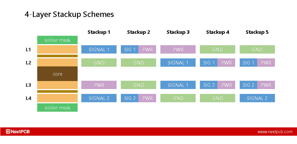
A common good start is the inner plane structure, where one layer is dedicated to ground and power, respectively. With a typical prepreg - core - prepreg lamination structure, traces sit close to ground or power reference planes, as in the first and second stackups in the figure, separated by a thin dielectric.
In stackup 1, digital signals should be routed on the top side (adjacent to GND), with slower signals grouped on the bottom layer, especially if multiple voltages are used. The power plane can be replaced with another ground layer (stackup 2) by implementing power rails in the signal layers, allowing for digital signals on both outer layers.
Despite having a ground and power plane adjacent to one another, the thick core dielectric renders the intrinsic plane capacitance ineffective for high-frequency decoupling, resulting in poor power integrity. Considering this separation is often 0.2mm in a standard 0.6mm board and exceeds 0.5mm in thicker PCBs, implementing an effective ground-power plane pair in a typical four-layer PCB has limited effectiveness at best.
A less common but worthy EMC alternative is the inner signal - outer plane structure (stackup 3 and 4). This forms a shielded cavity with high-speed signals routed as stripline, reducing both radiated emissions and susceptibility to external interference. With this structure, it is significantly easier to pass stringent EMC tests for FCC/CE compliance without metal shields or complex filtering. Stackup 4 is even better for EMI suppression, but severely limits routing space.
In this case, the thick core helps to reduce crosstalk between the adjacent signal layers; however, care should still be taken to minimize residue interference by employing orthogonal routing.
Another significant limitation is that components mounted on the outer sides would risk significantly breaking up the solid planes, so this structure is typically reserved for designs with very few components, such as simple filters.
Is cost a major factor in your designs? Make sure you utilize our standard stackups for the best cost performance.
6-layer boards offer even more design flexibility and performance enhancements for more complex designs. The benefits are profound, with more and more high-speed design guides such as memory modules, specifically recommending that boards have at least 6 layers.
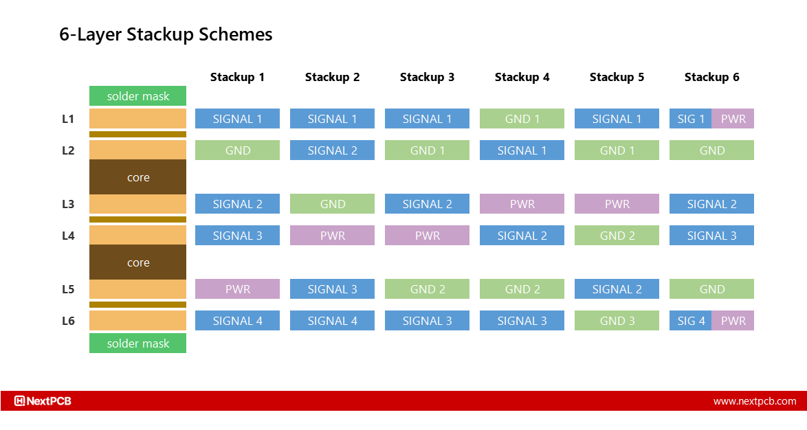
The most conventional 6-layer stackup, stackup 1, is shown in the above figure. It offers maximum routing space by adding two signal layers to the center of a 4-layer stackup. The ground and power planes offer shielding for inner signal layers L3 and L4 while providing an immediate reference plane for all four signal layers. However, the use of a single ground plane means the shielding capabilities are limited, and there is a high-inductance return path from L6 to ground. An alternative (stackup 6) is to route power on the outer layers to shorten the return path and offer better shielding at the expense of routing space and simplicity. Care must also be taken to avoid crosstalk between signals in the two inner layers.
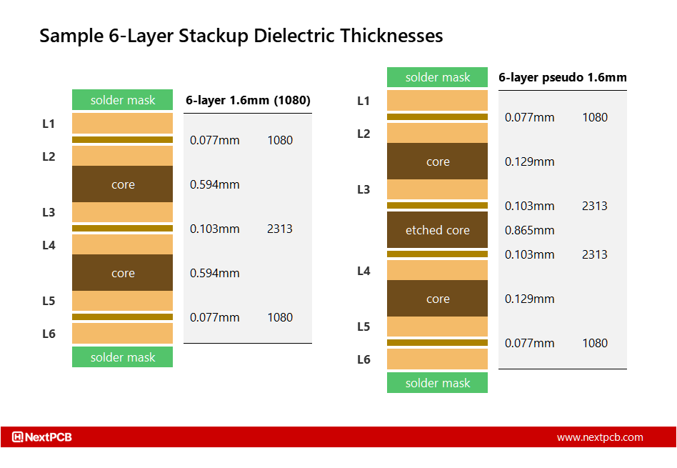
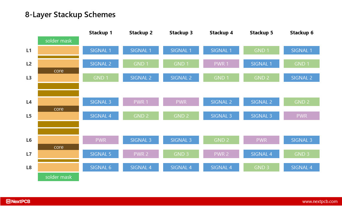
To remedy this, a pseudo 8-layer stackup can be used, which increases the spacing between L3 and L4 by adding an etched core - simply, another piece of thick dielectric. At the same time, the thicknesses of the other two cores are reduced, which can be exploited in PWR-GND pairs. As the name suggests, however, this is considered an 8-layer board in terms of manufacturing complexity, so designers should compare the advantages of a pseudo-8-layer board with a standard 8-layer stackup first.
Stackup 2 is an improvement that brings the two planes closer together for effective high-frequency decoupling. By taking advantage of the thin dielectric at the center of a standard 6-layer stackup, this configuration supports exceptional high-speed power integrity, reducing reliance on decoupling capacitors and suppressing noise. On the downside, however, the inner signal layers are separated from their references by thick cores, and the outer signal layers are adjacent to signal layers, not reference planes. This is the exact opposite of what we want for signal integrity and EMC.
Stackup 3 eliminates these problems by replacing a signal layer with a ground plane for additional shielding and ensures each signal layer sits next to a solid reference plane, while maintaining a PWR-GND pair.
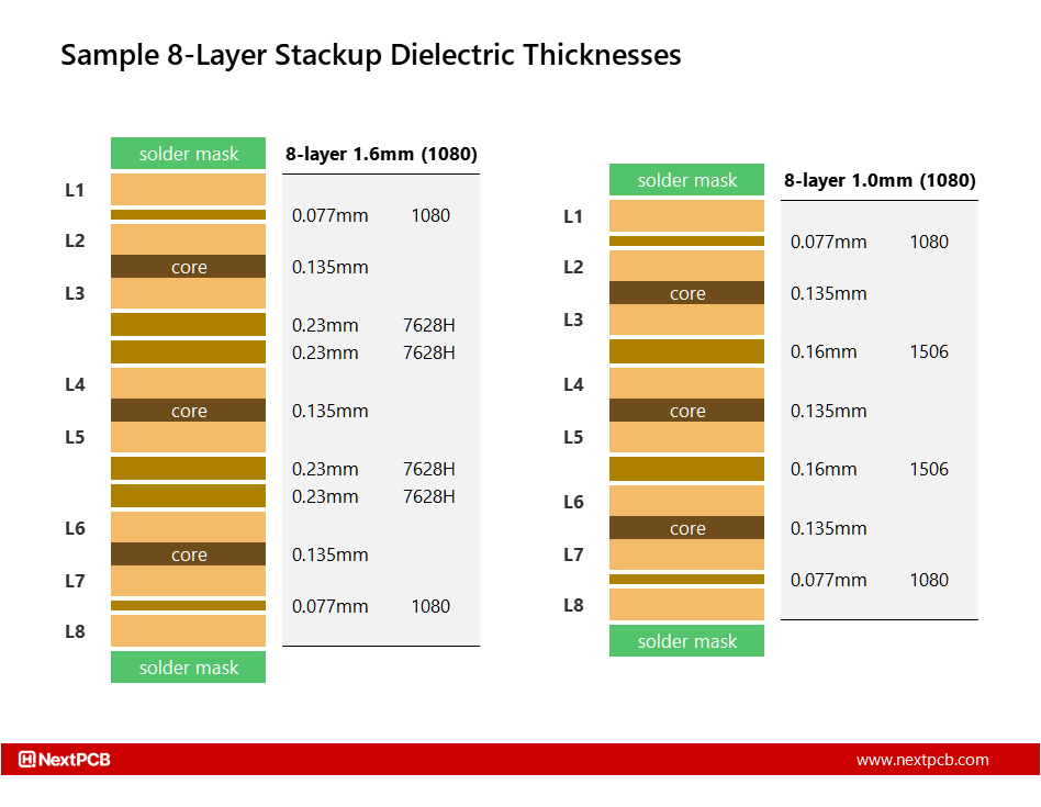
In a 6-layer stackup, the core layers are typically much thinner - we are now using two cores instead of one to make up the remaining thickness. The 1.0mm thick board in the figure below, 1.0mm thick board, the two cores are 0.294mm thick as opposed to 0.594mm in a 1.0mm 4-layer board. This is further reduced to 0.194mm in a 0.8mm-thick 6-layer board. The thinner the dielectric, the greater the plane capacitance. This configuration would also benefit from a pseudo-8-layer stackup, as this would push L3 away from any power plane splits in L4 and closer to the L2 ground plane, and the PWR-GND pair would be even closer together.
The only significant drawback of this stackup is potential copper imbalance, which is easily remedied by adding a ground or power copper pour to the empty areas on L3. This prevents the pour from acting as an antenna while maintaining structural balance.
Stackup 5 provides better decoupling and shielding at the expense of an outer signal layer. There is high decoupling between the central pair and the internal layer is encased in a ground cage. This configuration, however, leaves only two layers for routing and one side for mounting components.
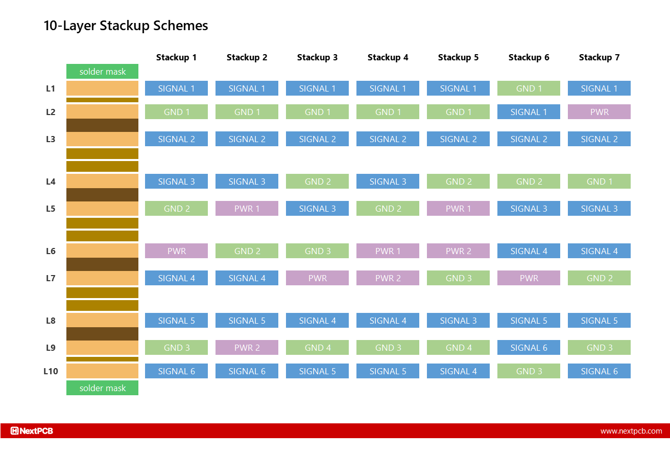
Despite significant advantages over 4-layer stackups, 6-layer stackups still struggle to achieve all our goals of ideal power integrity, signal integrity, circuit density, and structural balance all at once. Higher layer counts allow for more of the same coupling and isolation techniques that we have visited above, but with more freedom.
Stackup 1 combines the disadvantages of the first two 6-layer stackups in exchange for maximizing the number of signal layers. This configuration should only be used if the impedance and signal integrity requirements are low.
Stackup 2 is a vast improvement that adds a PWR-GND plane pair for robust power integrity and provides a reference plane for every signal layer. Stackup 3 further enhances EMC by sacrificing a dedicated power plane to create a shielded “ground cage” for exceptional EMI suppression and shorter return paths.
It is important to note that some 8-layer and higher order lamination structures use multiple stacked prepregs and thinner cores, effectively making core dielectrics thinner than prepreg areas. This can be taken advantage of for high-speed stackup design, as it allows symmetrical plane pairs either side of the centre as well as directly in the centre of the stackup, maintaining maximum symmetry. In thinner boards and higher layer counts, the thicknesses of all dielectric layers can easily fall below 0.2mm, great for tighter coupling and return path management.
Stackup 4 can be viewed as a direct improvement on the first 6-layer stackup. The additional layers are used to form two plane pairs and create an isolated stripline environment while maintaining perfect symmetry. Two layers are opened up for power.
Higher PCB layer counts offer more opportunities to strategically use thin dielectrics. In the stackup below, there is little difference between the core and prepreg dielectric thicknesses, allowing for tighter plane pair coupling and closer signal references. On the flipside, however, the closer separation provides poor isolation between adjacent signal layers. Therefore, careful planning is still required to 1) separate high-speed signal layers
In a typical workflow, designers would allocate their copper layers first, then find or create a stackup that works with this configuration. However, in a cost-sensitive environment, this is likely not the most sound approach, and can result in broken budgets or costly respins.
Real-world manufacturing constraints dictate feasibility, cost, and reliability. Consequently, effective stackup design requires a strategic balance where signal integrity, EMC, and cost are all prioritized, with trade-offs often necessary. A particular stackup may have its merits, but it may not be worth the extra manufacturing cost in the long term. NextPCB provides a selection of over 40 popular lamination structures to fit a variety of high-speed requirements at no extra charge. By configuring your stackup to use these structures, you can be sure your design will not incur additional last-minute fees and take advantage of quickturn costs and lead times.
Check out all our stackups via the impedance calculator, or learn more about our complete impedance control services.
How to use Standard PCB Stackups for Controlled Impedance
NextPCB PCB Impedance Control Services
NextPCB High-Speed PCB Manufacturing Services

Still, need help? Contact Us: support@nextpcb.com
Need a PCB or PCBA quote? Quote now


 Surface

