
 Surface


Julia Wu - Senior Sales Engineer at NextPCB.com

 NextPCB Capabilities
Printed Circuit Boards
NextPCB Capabilities
Printed Circuit Boards
 PCB Assembly
 Layer Buildup
 SMD-Stencils
 PCB Design-Aid & Layout
 Mechanics
 Quality
 Drills & Throughplating
 Factory & Certificate
 PCB Assembly Factory Show
Certificate
PCB Assembly Factory Show
Certificate
Support Team
Feedback:
support@nextpcb.com


Introduction
Modern HDI design pushes PCB real estate to its limits, and few techniques shift the design envelope as decisively as Via-in-Pad (VIP). By placing a filled-and-capped via directly in the component land—rather than using a dog-bone fanout—VIP unlocks routing channels under fine-pitch BGA/QFN packages, shortens current-return loops for cleaner SI/PI, and creates high-efficiency thermal paths from the die into internal copper planes. While VIP adds fabrication steps (fill, cure, planarize, copper cap) and tightens process control, it often lowers total system cost by enabling layer-count reduction and denser layouts that would otherwise be impractical.
This technical review distills VIP from first principles to factory realities. We clarify when VIP is essential (≤0.50 mm pitches, high-speed power delivery, thermal pads), how to size pads and holes against annular-ring and registration limits, and how filled/capped geometry preserves impedance at the pad. On the manufacturing side, we walk through resin-plugging and planarization controls, outline IPC-4761 Type VII and related IPC-2221/IPC-6012 guidance, and highlight failure modes—voiding, offgassing, and CTE-mismatch stress—that drive reliability and yield. Finally, we translate the trade-offs into actionable DFM rules and a capability-aligned checklist you can use with your fabricator.
> Recommend reading: PCB Assembly Capabilities | Quick-Turn Prototype to Volume Production
> Recommend reading: PCB Capabilities - NextPCB
Table of Contents
Modern electronics, driven by demands for miniaturization and increased functional density, necessitate complex Printed Circuit Board (PCB) architectures. Within this landscape, the vertical interconnect access, or via, transitions from a simple conductive hole to a critical high-performance component. Via-in-Pad (VIP) technology represents the most advanced solution for connectivity in space-constrained designs, fundamentally altering traditional PCB design rules and manufacturing processes.
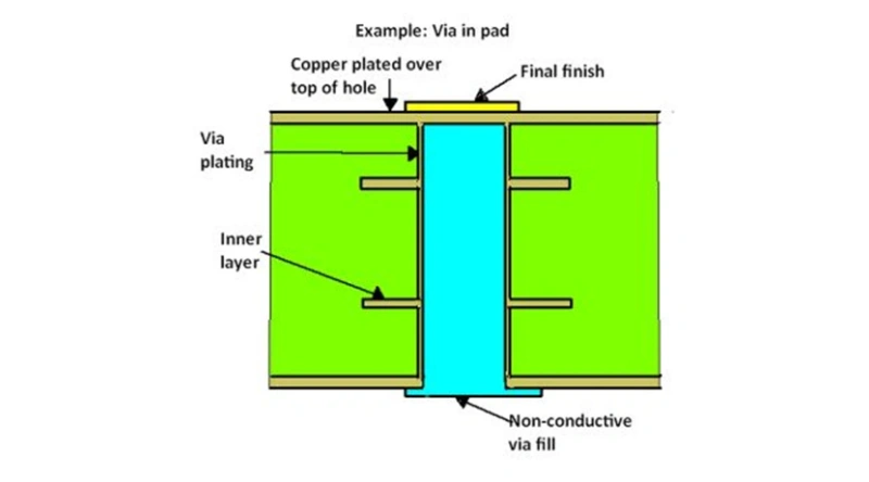
A Via-in-Pad (VIP) is defined as a design technique wherein a via is placed directly within the copper landing pad of a surface-mounted component. This approach stands in contrast to conventional methods, such as the "dog-bone" fanout, where a trace routes the signal from the pad to an adjacent, offset via. The structural necessity of VIP for reliability mandates that the drilled hole is typically filled with a specialized non-conductive epoxy, planarized to achieve flatness, and then plated (capped) over with copper. This rigorous process prevents short circuits and, crucially, avoids the detrimental effects of empty soldering caused by tin leakage or solder depletion during component assembly.
Vias are categorized by their depth and termination points: through-hole vias span the entire board thickness; blind vias connect an external layer to an internal layer; and buried vias connect two internal layers without appearing on the surface. VIP technology, particularly when used with high-density components, generally requires the highest tier of manufacturing complexity. The necessary addition of specialized steps—drilling, filling, planarization, and capping—significantly increases the processing requirements, often exceeding those of standard blind or buried vias.
Table I: Comparative Analysis of Advanced PCB Vias
|
Via Type |
Primary Application |
Manufacturing Complexity |
DFM Requirement (Key Constraint) |
Cost Implication |
|
Through-Hole Via (THV) |
Low-to-Mid density; Component mounting. |
Low |
High Aspect Ratio (Drill Depth/Diameter) |
Low (Baseline) |
|
Blind Via |
HDI (Layer reduction); External connection only. |
Moderate |
Aspect Ratio; Controlled Depth Drilling/Resin Depth |
Moderate |
|
Buried Via |
HDI (Layer reduction); Internal layer connection only. |
High |
Registration; Multiple Lamination Cycles |
High |
|
Via-in-Pad (VIP) |
Fine-pitch BGA/QFN; High-speed/Thermal. |
Highest |
Surface Planarity (Filling/Capping quality); CTE Matching |
Very High |
The primary driver for VIP adoption is the geometric challenge posed by modern Ball Grid Array (BGA) and Quad-flat No-leads (QFN) packages, especially those with fine-pitch arrays. As pin densities increase, traditional dog-bone routing becomes inefficient or physically impossible, as there is insufficient space between component pads for both a trace and an offset via pad. By placing the via directly under the component pad, VIP technology eliminates the surface trace entirely, creating significant space savings for component placement and subsequent routing.
This technology becomes mandatory for aggressive miniaturization. For BGA packages, VIP is generally considered essential for pitches of 0.5mm and smaller, and highly advantageous for optimizing layout efficiency in devices with pitches ranging up to 1.0mm. The adoption of VIP allows designers to utilize the maximum available surface area for component placement, enabling further routing channels and resulting in a smaller final package size.
Although the fabrication of VIP is inherently costly, requiring 8 to 10 additional steps in the PCB manufacturing flow, its utility must be viewed within the context of total system cost optimization. The ability of VIP to maximize component and routing density per layer often facilitates a reduction in the total layer count required for the PCB. In complex High-Density Interconnect (HDI) stackups, the incremental cost associated with adding even a few layers (e.g., moving from an 8-layer to a 10-layer design) frequently surpasses the additive cost incurred by implementing VIP processing across the board area. Therefore, by compressing the design vertically, VIP technology provides a crucial trade-off, delivering a net cost reduction when the final system complexity and density requirements are considered. This elevates VIP from a simple design feature to a strategic tool for minimizing overall product size and manufacturing expenditure for high-performance electronics.
In high-speed and high-frequency applications, maintaining signal integrity is paramount. VIP technology offers substantial benefits by optimizing the geometry of critical signal paths, specifically targeting the reduction of inductive effects and ensuring reliable decoupling near active devices.
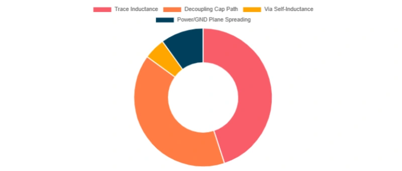
The use of vias inherently introduces discontinuities in the signal path, primarily in the form of self-inductance. Claims that VIP universally reduces via inductance require careful technical clarification. VIP technology does not inherently reduce the via’s intrinsic self-inductance, which typically hovers around 1nH. The quantifiable high-speed benefit of VIP stems primarily from the reduction of loop inductance. Loop inductance is the sum of all inductances along the current path, including the trace, the via, and the return path. By eliminating the surface trace required in a traditional dog-bone structure, VIP minimizes the overall current loop area. While the trace portion of the inductance (a few picohenries (pH)) is small compared to the via’s self-inductance, the reduction in the current loop area directly minimizes the adverse effects of transient voltage drop (L(di/dt)), which is critical for maintaining stable power delivery during high-speed switching events.
The most significant high-speed advantage VIP provides is the physical access it grants to critical decoupling locations. VIP allows the essential bypass (decoupling) capacitor to be placed directly adjacent to or even underneath the component package, minimizing the distance from the component power pin to the power/ground plane. This optimized placement ensures the shortest possible connection path, which is indispensable for ensuring the capacitor is effective at the highest switching frequencies. This ability to place the via directly onto the pad enhances grounding pathways, which is crucial for high-frequency components that require stable impedance and robust return paths.
For scenarios involving extremely fine-pitch components where routing channels remain congested, design for manufacturability (DFM) may involve placing the via slightly off-center within the pad. This strategy facilitates alternating rows of vias, allowing breakout traces to fit between pad rows while maintaining the advantages of the VIP structure. Designers should, however, be cognizant that even slight off-center positioning can subtly alter the local capacitance, which may necessitate careful simulation when dealing with extremely high-speed Radio Frequency (RF) signals.
> Recommend reading: The Ultimate PCB Routing Guidelines
The geometric requirements for high-speed signal integrity extend beyond inductance minimization and decoupling. A fundamental requirement for reliable high-speed transmission is maintaining consistent characteristic impedance throughout the transmission line. Any discontinuity in impedance, particularly at the connection point to the component, can cause signal reflections and degradation. Because a properly fabricated VIP is filled, planarized, and capped, it provides a perfectly flat, uniform surface right up to the component attachment point. This consistent geometry is essential for preserving the characteristic impedance of the signal path, effectively defeating performance limits often imposed by complex high-frequency PCB designs. The manufacturing requirement for surface planarity is, therefore, not merely a mechanical necessity for reliable soldering, but an electromagnetic necessity for maintaining signal quality.
> Recommend reading: Best 6-Layer PCB Stackups for Signal Integrity & Impedance Control
For power-intensive integrated circuits (ICs), such as high-core count BGAs and large QFNs, effective thermal management is essential for operational reliability and longevity. VIP technology provides a superior means of transferring thermal energy away from the heat source and into internal copper planes.
Copper possesses excellent thermal conductivity, making vias ideal thermal conductors in addition to their electrical function. When deployed beneath high-power components, these vias are specifically designated as "thermal vias." The primary function of a thermal VIP is to decrease the overall thermal resistance from the component's junction (the heat source) to the ambient environment (ΘJA). The VIP structure establishes a direct, low-thermal-resistance pathway connecting the heat source pad immediately to internal layers, which often serve as large heat sinks (e.g., dedicated ground or power planes).
This strategic use of thermal VIPs results in lower thermal resistance compared to methods that route heat horizontally away from the component pad before transitioning to the Z-axis (e.g., standard thermal stitching fields). By ensuring proximity to the component's heat source, VIP minimizes the distance heat must travel horizontally on the surface, maximizing the efficiency of vertical heat transfer and ensuring superior localized thermal performance.
> Recommend reading: PCB Thermal Design Basics (1): Substrate Material Selection
Thermal vias are critical for packages designed to leverage a central thermal pad, such as QFNs. In QFN packages, the exposed paddle is engineered to be the primary thermal conduit. This path, when properly soldered, significantly transfers heat away from the die (in some typical cases, carrying around 70% of the heat). When the exposed pad is effectively soldered to a large internal ground plane via an array of VIPs, the efficiency of heat transfer through this pathway is dramatically increased, potentially maximizing the vertical heat flow to figures exceeding 90% under optimized conditions.
Empirical studies confirm that thermal vias placed directly beneath the component's exposed thermal pad significantly enhance heat dissipation efficiency. The performance of the thermal path is proportional to the number and size of the thermal vias used, with researchers finding that increasing the quantity and diameter of thermal vias improves overall heat dissipation. Furthermore, implementing a square distribution layout for these thermal VIPs offers specific advantages in achieving thermal uniformity across the package footprint.
Designing effective thermal VIPs requires balancing multiple material parameters. While using more copper seems intuitively beneficial for heat transfer, designers and fabricators must exercise caution. Research indicates that excessive copper cap plating thickness can paradoxically increase the thermal resistance of the path, thereby hindering the component's ability to dissipate heat. The fabricator must therefore carefully control the copper deposition processes to ensure sufficient mechanical strength and coverage without compromising thermal performance. > Standard PCB Thickness – An Important Role in PCB Function
Furthermore, the materials used to fill the VIP structure are critical to its long-term reliability. The non-conductive epoxy fill must possess a Coefficient of Thermal Expansion (CTE) that is compatible with the surrounding materials (copper barrel and FR4 laminate). A significant CTE mismatch can introduce internal stresses within the via barrel or the surrounding laminate, potentially leading to mechanical failure during thermal cycling, which is common in high-power applications. Proper material selection for the fill ensures the structural integrity of the VIP throughout its operational lifetime.
The robust performance and space-saving attributes of VIP technology are achieved at the expense of manufacturing simplicity. Via-in-Pad is a high-cost, high-complexity process that requires stringent process control to guarantee reliability.
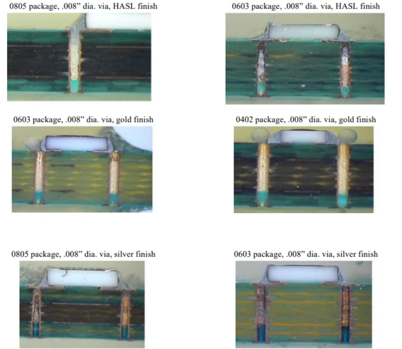
Picture cited from: https://www.electronics.org/system/files/technical_resource/E18%26S37-2.pdf
It is strictly mandatory to use filled and capped VIPs when placing vias directly under Surface Mount Technology (SMT) component pads. The failure to follow this requirement by leaving an open hole will lead to severe soldering defects. These defects typically manifest in two critical modes:
For fine-pitch components, especially BGAs down to pitch, achieving a perfectly flat, planar surface is mandatory for reliable component attachment. The complex fabrication process of filling and capping the via ensures this necessary flatness, eliminating surface bumps or deep dimples that would otherwise lead to placement errors or solder joint defects.
The introduction of VIP technology adds significant complexity to the standard PCB manufacturing sequence. This complexity is the primary driver of the increased cost and turnaround time.
>> NextPCB Assembly Capabilities
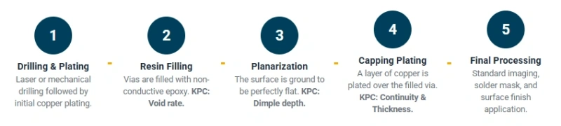
The typical fabrication sequence for creating a high-reliability, non-conductive filled VIP is organized into specialized process groups:
Critical Quality Control Point: Throughout the filling stage, the most critical quality factor is minimizing or eliminating internal air pockets, ensuring a low hole void rate to prevent offgassing failures during assembly.
HQDFM — Gerber & Assembly Auto-Check (DFM)
Manufacturing reliability for VIP structures centers on eliminating voids and managing thermal stress. If the via cavity is not perfectly filled during processing, trapped air pockets may remain. During the reflow soldering process, the intense heat causes this trapped air to expand—a phenomenon called offgassing or outgassing. This rapid expansion can cause structural damage or, more critically, force bubbles to travel through the molten solder, resulting in voids within the finished BGA solder joint, severely compromising reliability. The requirement for a completely filled cavity is thus a direct measure taken to prevent offgassing failures.
Furthermore, the long-term reliability of the VIP structure under thermal cycling hinges on the compatibility of the epoxy fill material's CTE with the surrounding materials. Incompatible CTEs lead to internal barrel stress and potential structural cracking or detachment, underlining the necessity of material engineering expertise in VIP fabrication.
The higher cost of VIP compared to standard PCBs is attributable primarily to three factors: process complexity, specialized materials, and reduced yield tolerance.
The multiple added manufacturing steps outlined above, including dedicated planarization and secondary capping, significantly increase labor and processing time.
Specialized materials, such as high-quality, low-CTE epoxy ink and the increased copper volume required for plating and capping, add to the base material cost.
Finally, the extremely tight tolerances required for achieving a perfect surface plane increase the potential for non-conformance if processes are not flawlessly executed, which in turn reduces manufacturing yields and drives up unit cost. It is crucial for designers to recognize that defects occurring within the BGA VIP region often render the PCB difficult or impossible to repair (rework), amplifying the financial consequences of manufacturing defects.
> PCB Assembly Design Guide: DFM, DFA, and Best Practices for 2025
To ensure manufacturability, reliability, and predictability in cost and cycle time, VIP designs must strictly adhere to industry standards, particularly those established by the IPC (Association Connecting Electronics Industries).
> NextPCB Promise the Product Safety with ISO 9001 UL Certifications
IPC-4761 defines standard methods for protecting vias. These methods are categorized by Type, outlining the required sealing and filling process:
For surface VIPs intended for SMT component attachment (BGAs, QFNs), high reliability mandates compliance with IPC-4761 Type VII. This classification ensures a robust, planarized surface, preventing issues like deep dimples or missing cap plating that could compromise the solder joint reliability.
The specific IPC designation profoundly impacts manufacturing complexity and cycle time. For example, opting for Type VII introduces 20 to 25 more processing steps than Type V and can increase the fabrication cycle time by 1 to 3 days. Consequently, specifying the precise IPC requirement for via protection is a critical step in DFM that directly influences both lead time and final fabrication cost.
> IPC Class 2 vs 3: The Differences in PCB IPC Standards
The reliability of a plated hole depends on the annular ring (AR), the copper distance between the finished hole wall and the edge of the pad. Adequate AR size is necessary to accommodate drill misregistration during fabrication and ensure sufficient plating integrity.
The minimum diameter of a surface pad (Dpad) for VIP applications must satisfy the general design formula for interconnect lands:
![]()
Where:
Note: Since the definition of Df and the value of C can differ based on whether the pad is on an external layer or an internal layer, designers must be cognizant of the differing tolerance requirements set by the manufacturer.
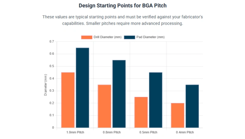
The physical requirements for VIPs scale aggressively based on the BGA pitch (e). Designers must coordinate the BGA pad geometry with the fabricator's capabilities for drilling and plating. The following table provides example dimensions to be used as a design starting point, which must be verified against the final manufacturer's Design for Manufacturability (DFM) guidelines.
Table II: Example Pitches and Recommended Dimensions for Fine-Pitch BGA Via-in-Pad
|
BGA Solder Ball Pitch (e) |
Min. Recommended Land (Pad) Diameter |
Via Finished Hole Diameter (V H ) |
Fanout Structure Preference |
|
1.0mm |
Standard (e.g., 0.5mm) |
0.25mm (10mil) |
VIP or Dog-bone |
|
0.92mm |
Standard |
0.25mm (10mil) |
VIP or Dog-bone |
|
0.5mm |
Min. BGA Pad ≥0.2mm |
0.10mm (4mil) |
Filled & Capped VIP (Essential) |
For highly aggressive pitches, such as 0.5mm, the required via finished hole diameter reduces to 4mil (0.10mm). This necessitates advanced fabrication techniques, often utilizing microvias (laser-ablated) rather than mechanical drilling, which further contributes to manufacturing complexity and cost.
Achieving reliable, high-yield VIP fabrication requires a partnership between the designer and a manufacturer possessing specialized, high-precision capabilities. NextPCB's facilities are explicitly optimized to handle the stringent requirements of VIP technology for fine-pitch HDI designs.
>> Recommend reading:
NextPCB's manufacturing specifications confirm a specialization in complex interconnect structures, stating optimization for "via-in-pad, dog-bone fanout and via aspect ratio balancing". This experience ensures that the multi-step VIP process is controlled with the necessary precision to deliver high-reliability components.
Key capabilities relevant to VIP implementation include:
Table III: NextPCB Manufacturing Capabilities for High-Reliability Via-in-Pad (VIP)
|
DFM Parameter |
NextPCB Capability/Specification |
Relevance to VIP Design |
|
Minimum Plated Hole Size (PTH) |
≥0.2mm (Single Side) |
Defines the smallest mechanical drill size usable for VIP. |
|
Plated Hole Size Tolerance |
±0.075mm |
Ensures tight control necessary for VIP reliability and component placement accuracy. |
|
Minimum Annular Ring (1oz Cu) |
3.5mil (≈0.09mm) |
Allows for maximum density, critical for fine-pitch BGA routing channels, surpassing typical IPC Level C minimums. |
|
Minimum BGA Pad Dimensions |
≥0.2mm |
Confirms capability for extremely aggressive fine-pitch component landings (e.g., pitch). |
|
VIP Optimization Status |
Optimized for via-in-pad fanout |
Confirms specialized process and dedicated experience. |
The ability to maintain a minimum annular ring of 3.5mil (0.09mm)for copper is a significant advantage, allowing designers to achieve greater routing channel density between pads than often possible with standard fabrication processes. This specification is particularly crucial for maximizing space efficiency around fine-pitch BGAs.
To leverage NextPCB's capabilities and ensure successful fabrication, designers must adhere to specific DFM rules:
Because VIP technology encompasses various complex processes—from mechanically drilled and non-conductive-filled vias to laser-ablated and fully copper-filled microvias—the resulting cost and performance can vary dramatically. Designers facing uncertainty in selecting the optimal technology for their specific application (especially involving high-frequency components or unique stack-ups) should engage directly with NextPCB's engineering team.
NextPCB's Computer-Aided Manufacturing (CAM) engineers can review the submitted design files to determine precisely which vias require filling and capping, mitigating fabrication risk and ensuring the most cost-effective solution is implemented. This consultative approach ensures that the finished PCB design maintains maximum density and performance while adhering to manufacturing best practices.
> You may also intersted in:
How to use Standard PCB Stackups for Controlled Impedance
PCB Layer Stackup: A Comprehensive Overview
As a global leader in HDI manufacturing services, NextPCB has compiled the most pressing Via-in-Pad (VIP) questions from PCB engineers across platforms like Reddit. Our senior process engineering team provides these authoritative answers.
A: When your component pitch is ≤ 0.5mm, traditional dog-bone fanouts consume too much routing space and can even block inner-layer traces. VIP technology reclaims this space by placing the via directly within the pad. Furthermore, for high-speed signals (10Gbps+) and high-power thermal designs, VIP significantly reduces parasitic inductance and improves heat dissipation efficiency.
A: It depends on the hole diameter and design requirements.
A: If manufacturing tolerances are loose (e.g., poor flatness or thin copper capping), the risk of assembly defects increases. NextPCB utilizes high-precision grinding processes to keep flatness deviation within a microscopic range, effectively eliminating cold solder joints or bubbles caused by uneven paste. We also recommend that designers maintain proper solder mask openings above the VIP.
A: At the CAD level, you simply place the via in the center of the pad. However, when exporting Gerber or ODB++ files, you must explicitly label them as "Vias to be plugged and capped." We strongly suggest providing a dedicated "Via Fill" layer to clearly identify which holes require VIP processing to avoid production confusion.
A: Yes, VIP adds several steps: specialized drilling, plugging, vacuum curing, grinding, and secondary plating. While the unit price is higher, VIP can often reduce the total layer count by 2–4 layers in complex HDI designs, which may offset the cost increase. At NextPCB, our automated resin-plugging lines keep lead times highly competitive.
A: This is a common misconception. For the vast majority of BGA signals, non-conductive resin is the preferred choice. Its Coefficient of Thermal Expansion (CTE) is more closely matched to the PCB base material, leading to higher long-term reliability. Conductive resin is generally reserved for rare cases with extreme current-carrying requirements.
Use our free PCB Via Current Calculator to estimate current-carrying capacity, resistance, voltage drop, and power loss — for both through-hole and buried/blind vias — based on the IPC-2221 conductor model.

Still, need help? Contact Us: support@nextpcb.com
Need a PCB or PCBA quote? Quote now

