Julia Wu - Senior Sales Engineer at NextPCB.com

Support Team
Feedback:
support@nextpcb.comIntroduction
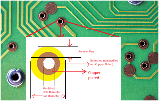
The traces need to route from one side of the board to the other side when designing a multi-layer PCB. The copper rings around the vias on the top and the bottom of the board are called annular rings. It is the area on the pad that surrounds the drilled and finished hole. The annular ring includes the copper-plated ring of the via and the pad area around the finished via. The annular ring is like a donut in the following picture.

The annular ring should be enough copper to form a secure connection between the copper traces and the vias in a multi-layer PCB. The primary function of the annular ring is to establish a connection between the via and the copper trace.
The width of the annular ring will affect the PCB design and manufacturing considerations. The width determines how much space the PCBs can move, or how much space the drill can move before the electrical connection is affected. A wide ring can ensure that even if the drill is off-center, the via will still be inside the pad and maintain functional connectivity.
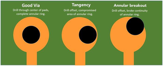
Sometimes the drilled via is not in the center of the pad. When a small ring touches the edge of the pad is called tangency, and an annular breakout means that the pad is not encircling the ring.

The tangency and the breakout of the annular usually are the result of the certain tolerance of the drills used in PCB manufacturers. If the PCB design cannot tolerate tangency or breakout, customers need to check the tolerance with the PCB manufacturers for suitable recommendations.
The ideal annular ring with holes is in the center of the pad, which can achieve the best connection between the vias and the layers. The following equation shows a perfect annular ring width.
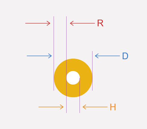
An annular ring width = (the diameter of the pad – the diameter of the hole) / 2

Let' s take the above picture like the example to calculate the width of the annular ring.
Eg:
Normally, the min-width of the annular ring is 0.15mm (6 mils). The drill size (CNC) is 0.2mm to 6.3 mm, which means the min drill size is 0.2mm, and the max drill size is 6.3mm. The hole size in this range does not need extra charges. Usually, engineers will confirm the standard tolerance of the annular ring with customers after receiving the order of PCB assembly prototype or PCB mass production, and provide the right suggestion to avoid the risk of a poor connection.
Still, need help? Contact Us: support@nextpcb.com
Need a PCB or PCBA quote? Quote now