
 NextPCB Capabilities
Printed Circuit Boards
NextPCB Capabilities
Printed Circuit Boards
 PCB Assembly
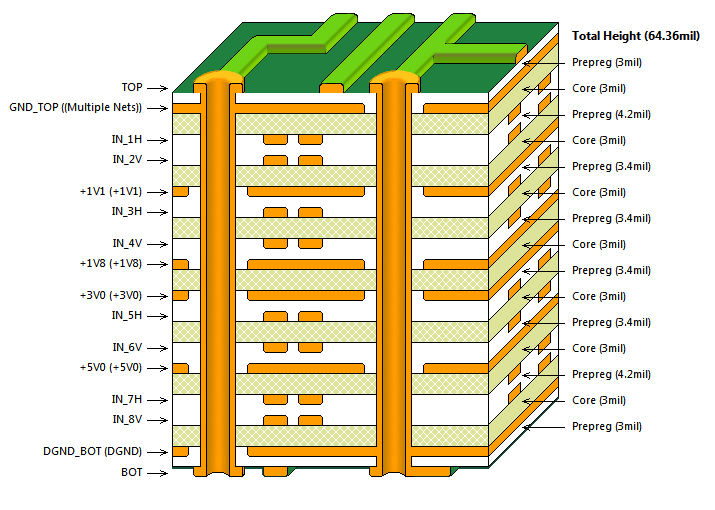
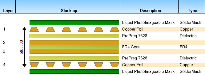
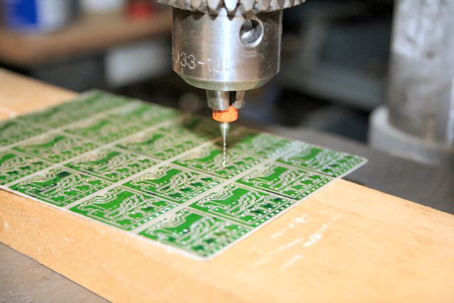
 Layer Buildup
 SMD-Stencils
 PCB Design-Aid & Layout
 Mechanics
 Quality
 Drills & Throughplating
 Factory & Certificate
 PCB Assembly Factory Show
Certificate
PCB Assembly Factory Show
Certificate
Support Team
Feedback:
support@nextpcb.com


A printed circuit board (PCB) stackup is the assembly of a PCB, which consists of many layers of insulating material and conductive channels. The stackup specifies how many layers there will be, what materials will be utilized, how thick they will be, and where the conductive paths will be located within each layer. Layers of copper and insulation are layered between each other to form the three-dimensional structure of a printed circuit board. Depending on the complexity of the circuitry, a PCB stackup could include anywhere from two to more than fifty layers. Attach electronic components or route power and ground signals, for example, would require a different layer of a printed circuit board (PCB).
The designers strategically place conductive routes in each layer to ensure maximum signal purity and minimum component interference. The materials used and their thickness can significantly affect the performance of a PCB stackup. Specialized materials like Rogers or Teflon, for instance, may be necessary for high-frequency circuits to minimize signal loss and preserve signal integrity. While designing a PCB stackup, one must take into account the electrical and mechanical needs of the circuit, as well as factors such as the size and shape of the board, and the cost and availability of materials. Careful PCB stackup design can improve the reliability and performance of a device.
A PCB stackup affects performance, reliability, and manufacturability. A good stackup improves signal integrity, electromagnetic interference, thermal management, and manufacturability.
PCB layers affect electrical performance, signal integrity, and product cost. Less material and manufacturing procedures enable simpler, cheaper PCB designs. A lower layer count may increase board size, routing complexity, and the inability to create high-density circuitry. PCB layers increase routing flexibility, signal integrity, and component density. Additional layers improve power and ground distribution, reducing EMI and circuit dependability. More PCB layers demand more material, processing, and inspection procedures, which increases production complexity and cost. Therefore, one must carefully choose the PCB layers based on electrical performance, signal integrity, and cost.
The number of layers in a PCB is an important design aspect that depends on the application.
Circuit layout and routing, material quality, and operating environment modify PCB signals.
Signals pass through PCB components, vias, and traces. These elements can alter signal impedance and capacitance, causing reflections, crosstalk, or signal deterioration.
Impedance matching, regulated routing, and signal integrity analysis help PCB designers reduce these impacts. Impedance matching reduces reflections and signals distortion by matching the signal source and transmission line impedances.
Controlled routing places key signals on selected PCB layers to avoid interference from other signals or power planes. Signal integrity analysis uses simulation techniques to forecast signal behavior in diverse conditions, allowing designers to optimize circuit layout and routing for the best performance. PCB materials can impair signal performance. High-quality materials with low dielectric constant and loss tangent reduce signal loss and distortion, enhancing circuit performance.
The circuit's surroundings can affect signal performance. PCB designers must consider high temperatures, humidity, and electromagnetic interference when designing the circuit. Hence, impedance matching, regulated routing, materials selection, and environmental considerations must be considered while building a PCB that consistently transmits signals. Designers can optimize these aspects to guarantee the circuit satisfies performance standards and works dependably in the intended application.
The number of components and their arrangement can greatly affect PCB component density.
Component density is the number of components that can fit on a PCB. In situations where board size is important, high component density can help designers fit more functionality into a smaller space. PCB stackup affects component density in numerous ways. For instance, adding layers to a PCB can improve component routing space, reducing board footprint and boosting component density. Stacking more layers in the same board thickness with a thinner dielectric material can help boost component density. However, adding layers increases manufacturing complexity and cost, which may not be necessary or desired for many applications. PCB designers must weigh component density, signal integrity, thermal management, and cost when choosing a stackup.
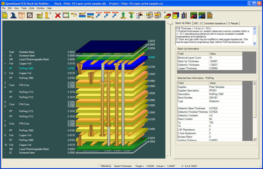
PCB stackup design determines board thickness. The number of layers, dielectric material, and copper thickness influence PCB thickness.
PCB mechanical stability, stiffness, and flexibility depend on board thickness. Thick boards decrease noise and EMI, preserving signal integrity. The application determines board thickness. Durable and reliable applications need thicker boards for mechanical stability. However, thicker boards require more material and manufacturing, increasing PCB cost. Board thickness impacts manufacturing. Thick boards demand more advanced equipment and methods to ensure quality and reliability.
Circuit layers determine board thickness. The PCB stackup design must optimize electrical performance, signal integrity, mechanical stability, and cost. PCB stackup design and board thickness are crucial design factors. Designers may guarantee the PCB meets electrical, mechanical, and financial criteria by choosing the right board thickness.
PCB stackup materials determine electrical performance, thermal management, and mechanical stability. Materials must meet electrical, thermal, and mechanical application criteria.
Most PCBs are made of FR-4 and their variants, which are inexpensive and have good electrical performance. High-frequency circuits may need Rogers, Teflon, or ceramic substrates to minimize signal loss and retain signal integrity. For high-power dissipation circuits, the thermal stability of PCB stackup materials is as crucial as dielectric characteristics. Aluminium, copper, and ceramic increase thermal management and circuit dependability. PCB stackup material thickness affects circuit performance. Thinner dielectric layers lower capacitance and signal integrity but increase electrical breakdown risk. Thicker copper layers increase current carrying capacity but also production costs.
Moisture resistance, chemical resistance, stiffness, and flexibility are also important when choosing PCB stackup materials. Lead-free solder must be used with the chosen materials.
PCB stackup copper weight is the thickness of its copper layers. Copper connects PCB components and circuits. While constructing a PCB stackup, copper weight impacts current-carrying capability and mechanical qualities. Copper weight is usually measured in ounces per square foot (oz/ft2) or grams per square meter (g/m2). Depending on the purpose, it can range from 0.5 to 5 oz/ft2.
Greater copper weight increases current-carrying capability but also board thickness and weight, which might affect mechanical stability and manufacturability. Thicker copper layers make the board harder to etch during manufacture. The thickness, current-carrying capacity, and mechanical strength of a PCB stackup affect the copper weight. High-current circuits employ thicker copper, while low-current circuits use thinner copper. PCB electrical performance and mechanical reliability depend on copper weight.
PCB stackup design depends on impedance control. Impedance, which resists electrical current in a circuit, depends on the signal frequency and properties. Impedance mismatches can cause signal distortion, reflections, and other signal integrity concerns in high-speed digital circuits, affecting performance. PCB designers utilize impedance control to keep crucial signal impedance within a specified range to mitigate these impacts. The thickness, dielectric constant, width, and spacing of the PCB stackup's insulating layers and conductive traces determine impedance. To obtain transmission line characteristic impedance, these parameters are changed.
Field solvers and simulation software can model PCB electrical activity and evaluate impedance control design. Data communication, networking, and computing use impedance-controlled PCBs for high-speed digital signaling.
PCB stackup design requires EMI and EMC shielding. EMI is the unintended generation, propagation, or reception of electromagnetic energy, while EMC is a device or system's capacity to operate in its electromagnetic environment without interference. Electromagnetic fields are shielded by conductive layers in the PCB stackup. Copper shielding layers can be on either side of the Board. A ground plane connects the shielding layer to undesired currents. EMI/EMC shielding efficacy depends on several aspects, including shielding material thickness and conductivity, stackup positioning, and signal trace routing. Shielded cables and connectors minimize EMI/EMC.
Designers must carefully arrange and route conductive traces and components to avoid EMI/EMC concerns. EMI/EMC considerations in a PCB stackup can assist guarantee that the finished product fulfills regulatory standards and works reliably in its intended environment.
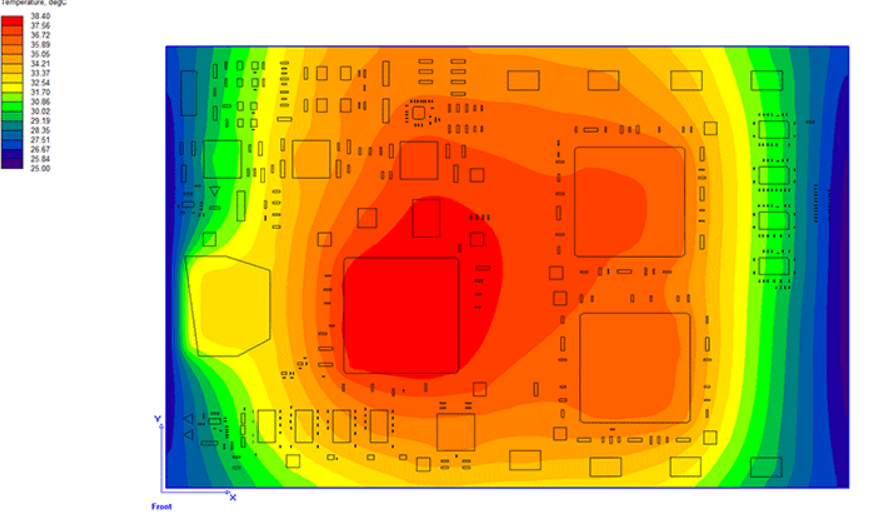
PCB stackup design requires thermal control. It involves dissipating component heat to prevent damage and preserve circuit reliability.
PCB stackup thermal performance can be managed in several ways. Copper or aluminum thermal management layers can be employed as heat sinks to dissipate component heat. These layers can transfer heat to the ground plane or other stackup layers.
Another method is to place heat-generating components in well-ventilated parts of the PCB layout. Individual components can use heat sinks to better dissipate heat. During design, the PCB stickup's thermal performance must be considered because excessive heat can damage components and cause circuit failure. Thermal simulations and testing can verify the stickup's thermal performance and meet application requirements.
Thermal management in PCB stackup design is crucial to product reliability and longevity.
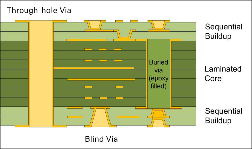
Through-hole vias connect all layers of the PCB. Blind vias connect an exterior layer to one or more interior layers without going through the PCB. Hidden vias connect PCB inner layers.
Board thickness, layer count, and component density determine through type. High-density PCBs use blind and buried vias to optimize routing and save space. They are harder and more expensive to make than through-hole vias. Therefore choosing a PCB stackup via type, examine the application
Drill size and aspect ratio are critical factors in the design of a PCB stackup. The drill size refers to the diameter of the holes drilled in the board, while the aspect ratio is the ratio of the drill depth to the drill diameter. The selection of drill size and aspect ratio affects the layer count, routing density, and mechanical stability of the board. Choosing the right drill size and aspect ratio is essential for ensuring proper electrical connectivity and signal integrity, while also maintaining the manufacturability and reliability of the board. Designers must carefully consider the layer count, board thickness, and material properties when selecting the appropriate drill size and aspect ratio for their PCB stackup.
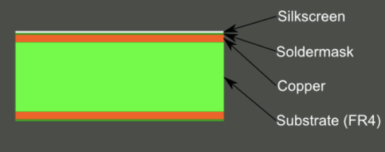
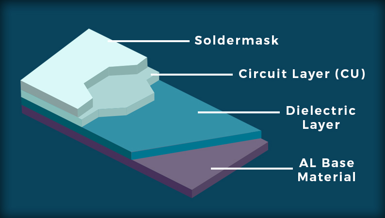
Soldermask and silkscreen protect and improve PCB readability. The solder mask layer coats the board to protect copper traces from oxidation and prevent solder bridging during assembly. It reduces unintentional shorts and opens, improving circuit dependability. The silkscreen layer, which is printed on top of the solder mask, identifies components and provides information about the board's layout and design. To improve the board's appearance, the silkscreen layer can add logos, part numbers, and other images. PCB functioning and quality depend on both layers.
PCB stackup design must consider tolerances and production restrictions. To ensure manufacturability and dependability, PCB tolerances must be considered. The design must consider the minimum drill size and aspect ratio, component spacing, and trace and space width. The materials must also be thick and stable for manufacture. To guarantee that the final PCB meets performance, reliability, and cost criteria, manufacturing tolerances and restrictions must be considered throughout the design. By designing the PCB stackup around these limits, the manufacturing process can be optimized and the product produced efficiently and cheaply.
The number of layers, material, the board size, and design complexity affect PCB stackup cost. PCB stackup costs can rise with more layers, specialty materials, and complex features like impedance control and heat management. A well-designed stack-up reduces the requirement for components and PCBs, saving money. To guarantee the product meets the criteria and is cost-effective, electrical performance and signal integrity must be balanced with stack-up cost. A proper study of cost aspects can optimize performance and cost.
PCB stackup design requires testability. A stackup designed for testability makes circuit testing and troubleshooting easier. Test points and vias in the stackup provide easy testing of crucial circuit nodes and components.
Impedance control and avoiding blind and buried vias in the stackup can also help assure reliable testing results. By listing the tests and their settings, a stackup test plan can help with testing and debugging. Testability in stackup design improves testing efficiency and accuracy, lowering circuit validation and debugging time and expense.
Finally, the PCB stackup affects printed circuit board performance, reliability, and cost. The number of layers, signal types, component density, board thickness, material selection, copper weight, impedance control, EMI/EMC shielding, thermal management, via types, drill size and aspect ratio, solder mask and silkscreen, tolerances and manufacturing constraints, cost, and testability must be considered when designing a PCB stackup. A well-designed PCB stackup can maximize electrical performance, signal integrity, thermal management, EMI reduction, signal loss, and circuit dependability by carefully selecting and ordering these aspects.
The routing flexibility, signal integrity, density, and cost of a PCB depend on its layer count. Higher layer counts improve routing flexibility and signal integrity but increase manufacturing complexity and cost. Lower layer counts simplify design and save costs but may increase board area and signal integrity. Designers must balance application electrical performance, signal integrity, and cost to optimize PCB stackup layers. The number of layers depends on the circuit's needs, the board's size and form, and materials and production costs.
PCB stackups are crucial to PCB design and manufacture. Designers can optimize performance, reliability, and cost by selecting and arranging layers and materials.
Still, need help? Contact Us: support@nextpcb.com
Need a PCB or PCBA quote? Quote now


 Surface

