PCB Assembly
Lolly Zheng- Sales Account Manager at NextPCB.com

 NextPCB Capabilities
Printed Circuit Boards
 Process Capabilities
 PCB Design-Aid & Layout
 Quality
 Drills & Throughplating
 Factory & Certificate
 PCB Assembly Factory Show
Certificate

Support Team
Feedback:
support@nextpcb.com


A transistor symbol shows three terminals and one arrow. In a bipolar junction transistor (BJT), the arrow is on the emitter: it points out for NPN and in for PNP. In a MOSFET, the arrow sits on the channel and points in for N-channel and out for P-channel. Letters tell you the pins: B, C, E for a BJT, and G, D, S for a FET.
This guide puts the common transistor symbols in one chart, then explains how to tell them apart, how to read the pins on a schematic, and what to check before the symbol becomes a footprint on your PCB.
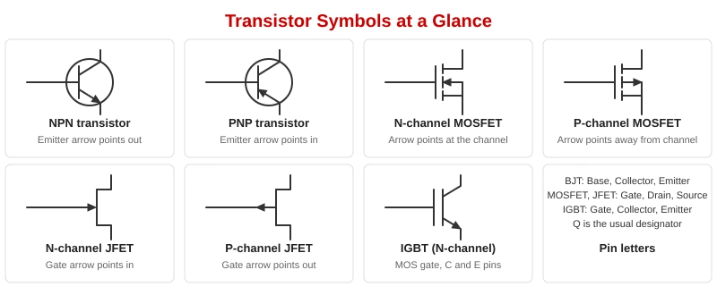
| Transistor type | What to look for in the symbol | Pins | Typical designator |
|---|---|---|---|
| NPN BJT | Circle optional; emitter arrow points out | Base, Collector, Emitter | Q |
| PNP BJT | Emitter arrow points in | Base, Collector, Emitter | Q |
| N-channel MOSFET | Gate plate, broken channel, arrow points toward the channel | Gate, Drain, Source | Q |
| P-channel MOSFET | Same, but the arrow points away from the channel | Gate, Drain, Source | Q |
| N-channel JFET | Solid channel, gate arrow points in | Gate, Drain, Source | Q |
| P-channel JFET | Solid channel, gate arrow points out | Gate, Drain, Source | Q |
| IGBT | MOS-style gate with a BJT-style collector and emitter | Gate, Collector, Emitter | Q |
Most libraries use Q for transistors, including MOSFETs and IGBTs. Some use T or TR, so follow your own library or your customer's standard.
The BJT symbol has a vertical bar for the base region. The base wire joins the bar from one side. The collector and emitter lines leave the bar at an angle, and the emitter line carries the arrow.
The arrow shows the direction of conventional current in the emitter. An NPN transistor switches on when the base is driven higher than the emitter, and a PNP when it is driven lower. For a closer look at how they differ, read the difference between PNP and NPN transistors, and for bias circuits see transistor biasing and amplifier design.
The circle around the symbol is optional. IEC style drawings usually show it, and many ANSI style drawings leave it out. Both mean the same part.
A MOSFET symbol has a gate plate that is separated from the channel by a gap, to show the insulated gate. The channel is drawn as three short segments for an enhancement-mode device, which is off at zero gate voltage. A depletion-mode MOSFET uses one solid channel line, because it conducts at zero gate voltage.
In most low-side switch circuits the source goes to ground and the drain goes to the load. See how a MOSFET works for the working principle and the IRFZ44N guide for a common example.
A JFET symbol has a solid channel line and a gate arrow. The arrow points into the channel for N-channel and out of it for P-channel. A JFET conducts at zero gate voltage, so it is normally on. For the basics of field-effect devices, see what a field-effect transistor is.
An IGBT is drawn with a MOS-style gate on the left and a BJT-style collector and emitter on the right. It is used in higher-voltage power switching such as motor drives and inverters. Its pins are gate, collector and emitter.
A Darlington pair is drawn as two transistors joined together, with the emitter of the first feeding the base of the second. The pair behaves like one transistor with high current gain. See a high-current motor driver using Darlington pair transistors for an example.
The symbol shows function, not pin position. The same transistor in a different package can have its pins in a different order, so always check the datasheet pinout. See transistor pinout and the BC547 guide for examples.
Related symbols are covered in our guides to diode symbols, resistor symbols and capacitor symbols. For the full set, see PCB schematic symbols and electronic component symbols.
Look at the emitter arrow. It points out for NPN and in for PNP.
A gate plate separated from a channel by a gap, with drain and source terminals. The channel arrow points in for N-channel and out for P-channel.
Base, collector and emitter, the three pins of a bipolar transistor.
Gate, drain and source, the three pins of a FET.
An enhancement-mode MOSFET has a broken channel line. A depletion-mode MOSFET has a solid channel line.
No. It is optional and the part is the same with or without it.
To read any transistor symbol, find the arrow first, then check which way it points and which terminal it sits on. Then confirm the pin names against the datasheet before you build the footprint.

Still, need help? Contact Us: support@nextpcb.com
Need a PCB or PCBA quote? Quote now