
 NextPCB Capabilities
Printed Circuit Boards
NextPCB Capabilities
Printed Circuit Boards
 PCB Assembly
 Layer Buildup
 SMD-Stencils
 PCB Design-Aid & Layout
 Mechanics
 Quality
 Drills & Throughplating
 Factory & Certificate
 PCB Assembly Factory Show
Certificate
PCB Assembly Factory Show
Certificate
Support Team
Feedback:
support@nextpcb.com


There are numerous sizes and forms for transistors. The bipolar type and the field effect are the two primary types. In this post, we'll mostly concentrate on the bipolar variation. Little electronic components known as transistors serve two fundamental purposes. It has the ability to switch on and off circuits and magnify signals.
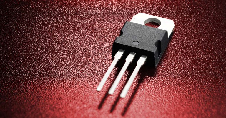
A resin case surrounds tiny, low-power transistors to help safeguard the interior components. Higher power transistors, however, will have a partially metal shell to help dissipate the heat produced, as this will eventually harm the components. These metal body transistors, typically linked to a heat sink, help eliminate the extra heat.
As an illustration, the MOSFET transistors inside this DC bench power supply are mounted to substantial heat sinks. With just 1.2 Amps of current flowing, the components soon reach 45 degrees Celsius (or 113 degrees Fahrenheit) without the heatsink. The more the current flows, the hotter it will get. However, we can just utilize resin body transistors, which do not require a heat sink, for electronic circuits with tiny currents.
Wording on the transistor's body provides the component number we need to locate the manufacturer's datasheet. Checking these sheets is essential since each transistor has a specified maximum voltage and current it can withstand.
A transistor has one circuit component all by itself. Simple electronic switches are made using transistors in tiny quantities. These are the fundamental components of integrated circuits (ICs), which are silicon microchips baked with many transistors coupled by circuitry.
Transistors are used in great quantities to build microprocessors, with millions of them packed into a single integrated circuit (IC). Also, they power the memory chips in computers and the memory storage units in MP3 players, smartphones, cameras, and video games. Nearly all integrated circuits (ICs), which are a component of every electronic device, contain transistors.
In low-frequency, high-power applications, such as power-supply inverters that change alternating current into direct current, transistors are also employed. Transistors are also utilized in high-frequency circuits that produce radio waves, such as oscillator circuits.
Kind of like a diode's extension, transistors are semiconductor components. In certain respects, transistors are merely two diodes connected at their cathodes (or anodes):
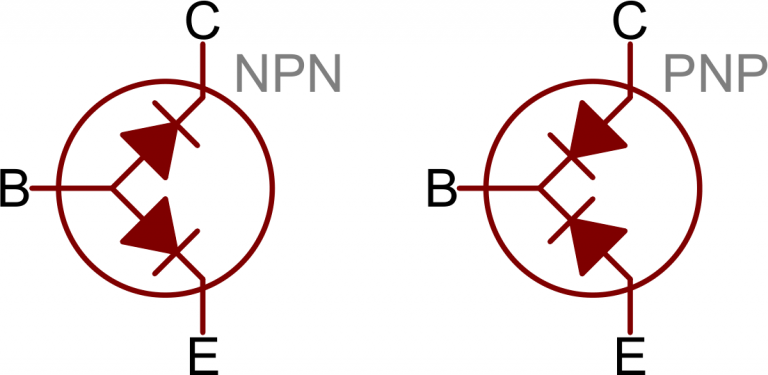
The key component in this circuit is the diode that connects the base and emitter because it indicates the desired direction of current flow via the transistor by matching the arrow's direction on the schematic symbol.
(This model comes in handy when testing transistors. You can test for the existence of those "diodes" by measuring across the BE and BC terminals using a multimeter's diode (or resistance) test function.)
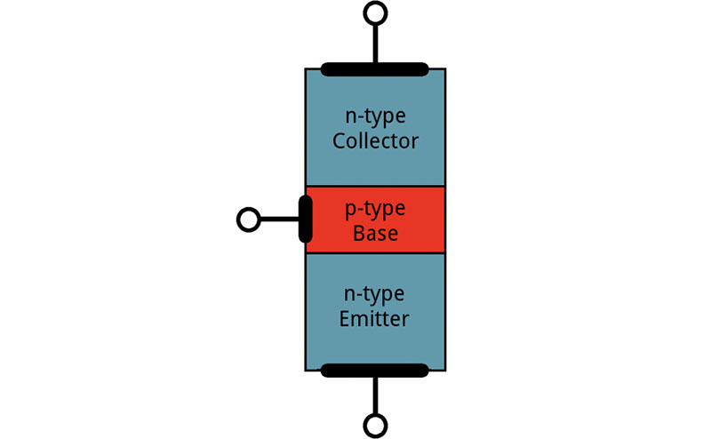
Three separate layers of semiconductor material are stacked together to create transistors. Doping is the process of adding extra electrons to some of those layers while depleting electrons from others (doped with "holes" — the absence of electrons). Because electrons have a negative charge, a semiconductor material with additional electrons is known as an n-type, while one with excess electrons removed is known as a p-type (for positive).
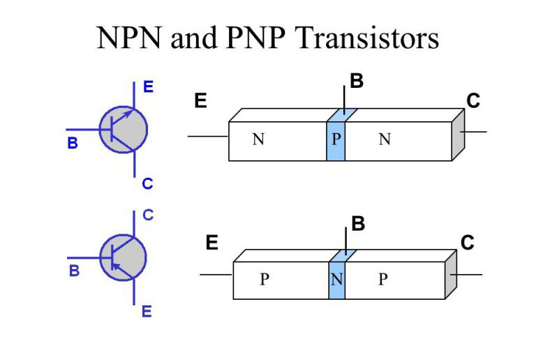
Typically, there are two types of transistors: NPN and PNP. The common housing options for these two types of transistors are plastic or metal. The transistor's front side is flat when it is in a plastic casing, and the pins are possible to identifiable serially. Allow the flat side to be facing you when you begin to count the pins.
The Collector, Base, and Emitter are typically the first, second, and third pins for NPN transistors, respectively. CBE is the configuration as a result.
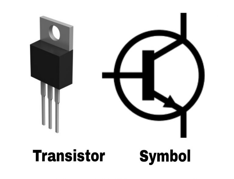
The situation is reversed with PNP transistors, though. The Emitter is the first pin, the Base is the second pin, and the Collector is the third pin.
The pins are arranged in a circular pattern when a metal case is used for the transistor. Look for a tab on the transistor's ring to identify the pins in this case. The Emitter pin on NPN transistors is the one that is closest to the tab. The Collector is located on the pin across from the Emitter, and the Base is located on the middle pin.
The emitter, denoted by the letter E, has a medium size and is strongly doped because its main job is to provide a large number of majority carriers to maintain the electricity flow. Since it emits electrons, it is known as the emitter.
The middle terminal between the emitter and the collector is known as the base and is denoted by the letter B. It is light-doped and thin. The carriers are passed from the emitter to the collector as its primary function.
The carrier that starts to flow from the emitter via the base get collects at the collector, that represents by the letter C. It is bigger than the emitter and base and moderately doped.
The PNP transistor operates in the opposite manner. The Collector is the pin that is closest to the tab, the Emitter is the one that is on the other side, and the Base is the pin in the middle.
We want you to imagine water flowing through a pipe in order to comprehend how a transistor operates. It runs freely through the pipe until we block it with a disc. We can now use a pulley to move the disc if we link a smaller pipe to the larger one and install a swing gate within the smaller pipe. More water is possible to flow through the main pipe the further the swing gate opens. An insignificant amount of water won't be sufficient to open the swing gate because it is somewhat heavy. It takes a specific volume of water to push the gate to open.
The valve opens more as more water flows through it, increasing the amount of water that may flow into the main pipe. In essence, this is how an NPN transistor operates.
You may already be aware that we employ conventional current while designing electrical circuits. So, we suppose that in this NPN transistor circuit, the current travels from the positive battery terminal to the collector and base pins and then exits the emitter pin. We always build our circuits in this direction.
But that's not what's happening right now. Actually, a battery's electrons move from the negative to the positive. Joseph Thompson conducted some tests to both discover the electron and demonstrate that electrons flowed in the opposite direction, and his findings demonstrated this. As a result, in practice, electrons move from the negative into the emitter before leaving through the collector and base pins. This is identifiable as the electron flow.
mainly there are two types of transistors available in the domain of electronics. They are possible to identify as follows;
One of the most popular types of transistors is the BJT, which can be either NPN or PNP. The emitter, base, and collector are the three terminals that make up a BJT. A BJT may magnify an electrical signal or turn current on or off by connecting these three layers.
A current flow get produce with the movement of electrons and holes, two different types of electrical charge. The base-collector junction of the BJT is normally reverse-biased with a high resistance, while the base-emitter junction is forward-biased with a very low emitter resistance.
Conduction occurs through holes or the lack of electrons in a PNP-type BJT. The emitter current is marginally greater than the collector current. Changes in the latter impact the former. From the emitter to the collector, the base regulates the current flow. In this instance, the emitter releases holes, which the collector then gathers.
Electrons move from the emitter to the base, and they meet at the collector in an NPN-type BJT. As a result, regular current travels from the collection to the emitter. The base regulates how many electrons the emitter emits.
The three terminals of a field-effect transistor (FET), known as the source, drain, and gate, are comparable to the emitter, collector, and base of a BJT, respectively. The n-type and p-type silicon layers design differently in the FET than they are in the BJT. Layering them with metal and oxide (MOSFET) is a way of forming the metal-oxide-semiconductor field effect transistor
Field effect, as used in FETs, is an effect that permits current to flow and turns on the transistor. The p-type gate that separates the n-type source and drain has holes that prevent electrons from passing through it. However, the creation of an electric field by applying a positive voltage to the gate allows electrons to go from the source to the drain. The field effect that results from this makes it easier for current to flow through the FET.
Low-noise amplifiers, buffer amplifiers, and analogue switches frequently employ FETs. The metal-semiconductor field-effect transistor (MESFET) is frequently good for high-frequency applications like microwave circuits.
The following are examples of other transistor types:
Still, need help? Contact Us: support@nextpcb.com
Need a PCB or PCBA quote? Quote now


 Surface

