
 Surface


Julia Wu - Senior Sales Engineer at NextPCB.com

 NextPCB Capabilities
Printed Circuit Boards
NextPCB Capabilities
Printed Circuit Boards
 PCB Assembly
 Layer Buildup
 SMD-Stencils
 PCB Design-Aid & Layout
 Mechanics
 Quality
 Drills & Throughplating
 Factory & Certificate
 PCB Assembly Factory Show
Certificate
PCB Assembly Factory Show
Certificate
Support Team
Feedback:
support@nextpcb.com


A MOSFET (metal-oxide-semiconductor field-effect transistor) works by using a voltage applied to its gate to control the flow of current between its source and drain terminals — without the gate drawing significant current itself. This makes MOSFETs the switching backbone of everything from power amplifiers to microprocessors.
MOSFET is used in a wide range of applications, from power amplifiers to microprocessors. Understanding the structure, functioning, and characteristics of MOSFETs is essential for any engineer or electronics enthusiast.
This article will provide you with a comprehensive guide to MOSFETs. We will cover the following topics:
The MOSFET, or metal-oxide-semiconductor field-effect transistor, is a crucial component in modern electronics. As a type of transistor, MOSFETs regulate and amplify electrical signals, using a metal gate insulated from the semiconductor material to control the flow of current between the source and drain regions.
MOSFETs come in two main types: enhancement mode and depletion mode, each suited to a different purpose. Due to their high input impedance, MOSFETs are highly efficient, requiring minimal current from the source to alter gate voltage. Their versatility allows for use in low-power applications as well as high-frequency switching, making them an essential part of many electronics projects.
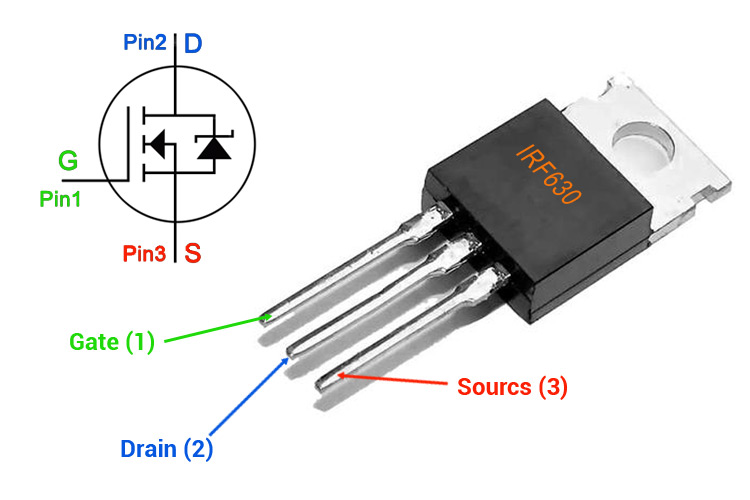
At their core lies the source-drain-gate structure – three distinct regions fabricated on top of a semiconductor substrate usually made out of silicon.
The source and drain regions are doped with impurities to create a high concentration of either electron (n-type) or holes (p-type) within the substrate. The gate region is created by depositing a thin layer of metal, such as aluminum or copper, onto the surface of the substrate. Hence the metal layer is then separated from the substrate by an insulating oxide layer, typically made of silicon dioxide (SiO2).
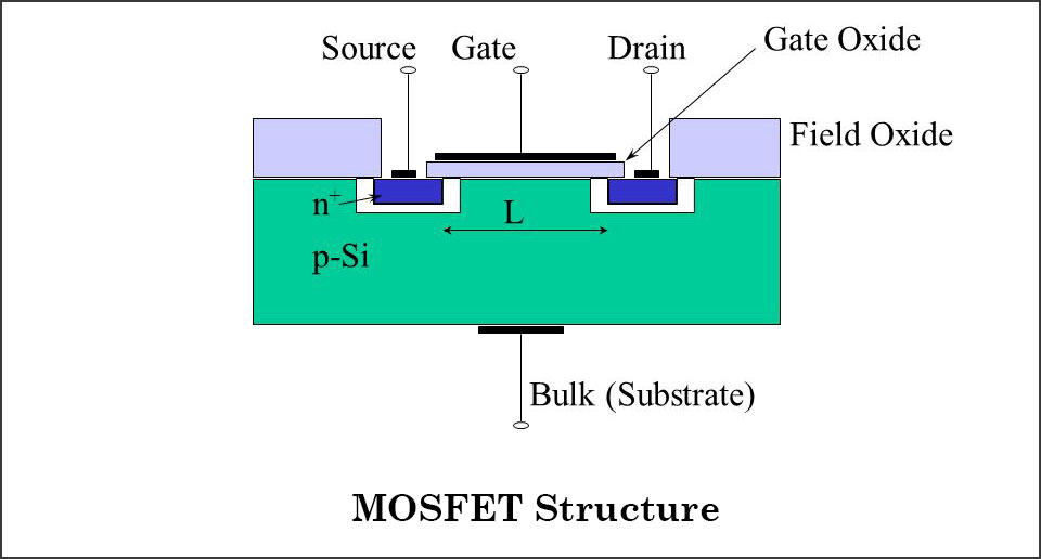
During fabrication, engineers carefully control the thickness of the oxide layer to ensure the proper operation of the MOSFET.
The oxide layer acts as a dielectric material and allows the gate to control the flow of current between the source and drain regions.
The MOSFET structure is possible to divide further into three different regions: the channel region, the depletion region, and the inversion layer.
The channel region is the region between the source and drain regions, and it contains a small number of free-charge carriers. When the gate voltage is zero, it creates a depletion region by depleting the channel region of charge carriers.
Applying a positive voltage to the gate generates an electric field that draws electrons from the source and drains regions toward the interface between the oxide layer and the substrate. This accumulation of electrons forms an inversion layer, which allows current to flow between the source and drain regions.
Controlling the voltage applied to the gate determines the amount of current flowing between the source and drain regions. The width and depth of the inversion layer are possible to regulate by adjusting the gate voltage, thereby allowing control over the resistance between the source and drain regions.
The MOSFET structure consists of three main regions: the source, drain, and gate. In the absence of a gate voltage, the channel region between the source and drain regions depletes charge carriers because of the separation of the gate from the substrate by an insulating oxide layer. Applying a gate voltage creates an inversion layer that enables the flow of current between the source and drain regions. The voltage applied to the gate controls the amount of current flowing between the source and drain.
There are several types of MOSFETs that are commonly applied in electronics. Some of the most common types of MOSFETs include:
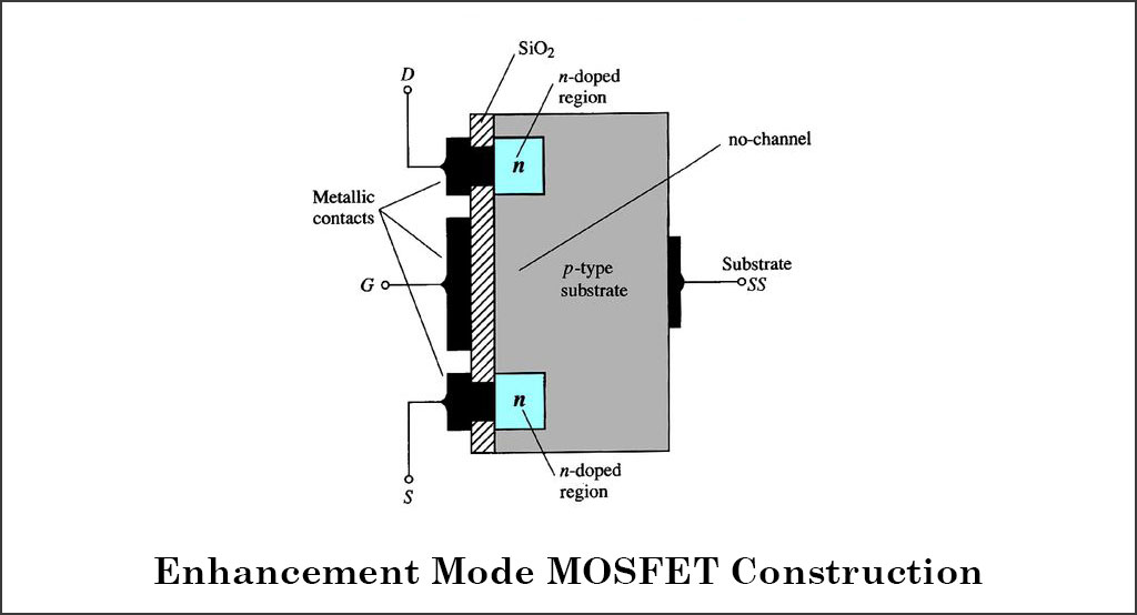
These MOSFETs have a normally-off channel between the source and drain, which is possible to turn on by applying a positive voltage to the gate. Enhancement-mode MOSFETs are widely applicable in power electronics and digital circuits.
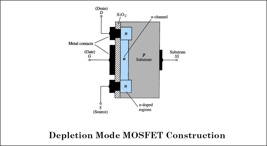
These MOSFETs have a normally-on channel between the source and drain, which is possible to turn off by applying a negative voltage to the gate. Depletion-mode MOSFETs are commonly applicable in low-noise amplifier circuits and voltage regulators.
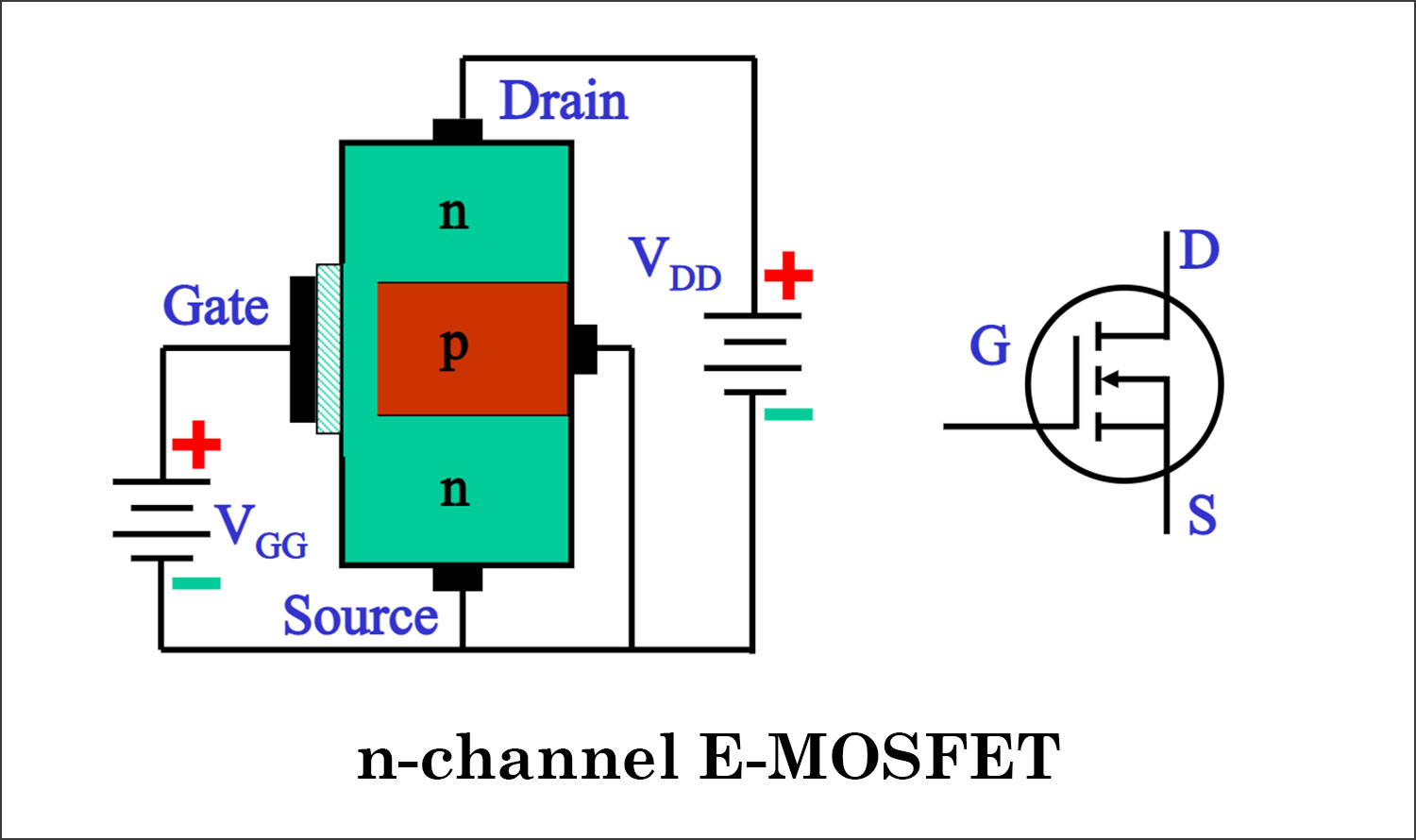
These MOSFETs have an n-type channel between the source and drain, which means that electrons are the majority carriers. N-channel MOSFETs are commonly applicable in low-side switching applications, where the source is in a connection with the ground.
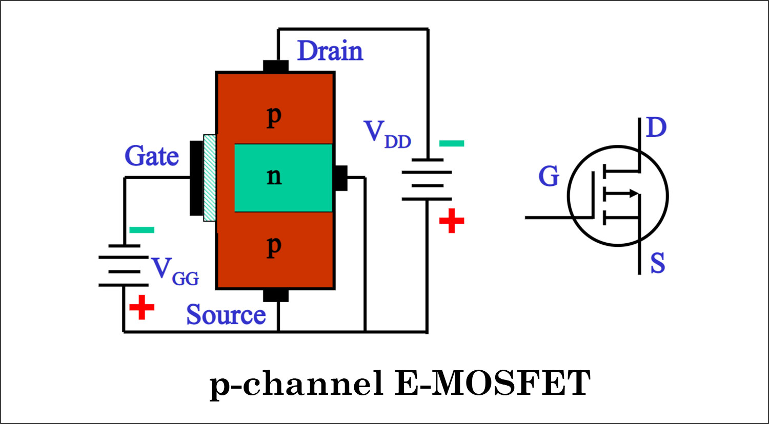
These MOSFETs have a p-type channel between the source and drain, which means that holes are the majority carriers. P-channel MOSFETs are commonly applicable in high-side switching applications, where the source is in a connection with the power supply.
CMOS circuits use both n-channel and p-channel MOSFETs to achieve low power consumption and high noise immunity. CMOS circuits are commonly applicable in digital logic circuits and microprocessors.
MOSFETs with different channel lengths and widths are possible to use to achieve different electrical characteristics, such as faster switching times or higher current ratings. MOSFETs are versatile devices that are possible to use in a wide range of electronic applications, and the choice of MOSFET type will depend on the specific requirements of the circuit.
The function of MOSFET is reliant on the mechanism by which the gate voltage manipulates the current flow between the source and drain regions.
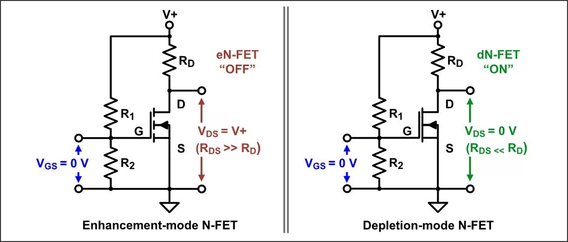
In an enhancement-mode MOSFET, the channel between the source and drain is normally off when there is no voltage applied to the gate. Accordingly, a positive voltage is applied to the gate, it creates an electric field that attracts electrons from the source and drains regions toward the oxide layer, creating an inversion layer that acts as a conducting channel.
The width and depth of this channel depend on the gate voltage. As the gate voltage increases, the channel becomes wider and deeper, allowing more current to flow between the source and drain regions. Conversely, as the gate voltage decreases, the channel becomes narrower and shallower, reducing the amount of current flowing between the source and drain regions.
In a depletion-mode MOSFET, the channel between the source and drain is normally on when there is no voltage at the gate. When a negative voltage is at the gate, it creates an electric field that depletes the channel of charge carriers, reducing the amount of current flowing between the source and drain regions.
As the gate voltage becomes more negative, the depletion region becomes wider and deeper, reducing the amount of current flowing between the source and drain regions. Conversely, as the gate voltage becomes less negative, the depletion region becomes narrower and shallower, allowing more current to flow between the source and drain regions.
In both types of MOSFETs, the gate voltage controls the flow of current between the source and drain regions, but the direction of the change in current with respect to the gate voltage is the opposite for enhancement mode and depletion mode MOSFETs.
One of the advantages of MOSFETs is that they have a very high input impedance, which means that they do not draw much current from the source when the gate voltage is varying. This makes them ideal for use in applications where low power consumption is important. MOSFETs are also able to operate at high frequencies, making them suitable for use in high-speed switching circuits.
MOSFET biasing refers to the process of setting the voltage and current levels at the MOSFET terminals to achieve the desired operation of the device. Proper biasing is critical for achieving optimal MOSFET performance and avoiding device damage.
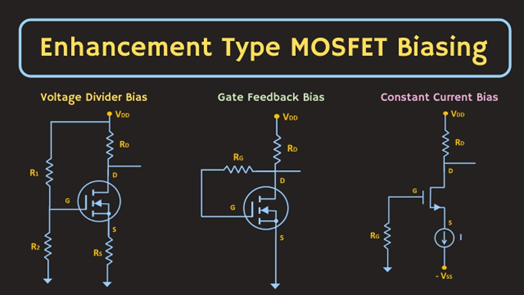
There are three common biasing techniques used in MOSFET circuits:
Therefore, it's important to note that MOSFETs are voltage-controlled devices, meaning that changes in the gate voltage can cause significant changes in the MOSFET current. Therefore, careful attention must be paid to the MOSFET biasing to ensure that the device is operated within its safe operating limits. Some factors that need to be considered while biasing a MOSFET include the maximum voltage and current ratings of the device, the required operating temperature range, and the frequency of operation. Proper biasing of MOSFETs can improve their reliability, performance, and overall efficiency.
MOSFETs exhibit several key characteristics that determine their performance in electronic circuits. Some of the most important MOSFET characteristics include:
Engineers choosing between a MOSFET and a bipolar junction transistor (BJT) are really choosing between voltage control and current control. The table below summarizes the practical differences that drive that decision.
| Characteristic | MOSFET | BJT |
|---|---|---|
| Control terminal | Gate (voltage-controlled) | Base (current-controlled) |
| Input impedance | Very high | Relatively low |
| Switching speed | Faster, better for high-frequency circuits | Slower due to minority carrier storage |
| On-state power loss | Lower at low voltage, governed by RDS(on) | Governed by VCE(sat), can be lower at high current |
| Thermal stability | Generally better, negative temperature coefficient of RDS(on) | Prone to thermal runaway without care |
| Typical applications | Power switching, DC-DC converters, digital logic | Audio amplification, analog signal processing |
In short, MOSFETs generally win on switching speed, power efficiency, and drive simplicity, which is why they dominate in modern power electronics and digital circuits, while BJTs still hold their ground in certain analog and audio applications where their gain characteristics are preferred.
A MOSFET acts as a voltage-controlled switch or amplifier: a voltage on the gate terminal controls current flow between the source and drain, without the gate drawing meaningful current.
The four main types are enhancement-mode N-channel, enhancement-mode P-channel, depletion-mode N-channel, and depletion-mode P-channel MOSFETs. CMOS designs combine N-channel and P-channel devices together.
A quick check uses a multimeter in diode-test mode to verify the gate is isolated from the source and drain, then confirms the channel conducts once the gate threshold voltage is applied and stops conducting once it is removed.
The gate is separated from the channel by a thin insulating oxide layer, so almost no DC current flows into the gate. This is what gives MOSFETs their very high input impedance compared to BJTs.
Yes. A MOSFET is a type of field-effect transistor, alongside JFETs. Unlike a bipolar junction transistor (BJT), which is current-controlled, a MOSFET is voltage-controlled through its insulated gate.
Finally, MOSFETs (Metal-Oxide-Semiconductor Field-Effect Transistors) are essential components in modern electronic circuits. They offer several advantages over other types of transistors, including high input impedance, low power consumption, and fast switching speeds. MOSFETs come in various styles, including enhancement-mode and depletion-mode MOSFETs, and they exhibit several key characteristics that determine their performance, such as RDS(on), VGS(th), CGS and CGD, VDS, ID, and thermal resistance.
Proper biasing of MOSFETs is critical for achieving optimal performance and avoiding device damage. The process of MOSFET biasing is possible to achieve through various methods such as Voltage Divider Biasing, Feedback Biasing, or Constant Current Biasing. The selection of the appropriate biasing method will depend on the specific requirements of the circuit. It's important to consider several factors when selecting and biasing MOSFETs, including the maximum voltage and current ratings of the device, the required operating temperature range, and the frequency of operation.
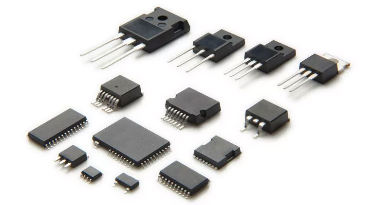
If your design calls for MOSFETs alongside other power components, NextPCB's PCB assembly service can help take your MOSFET-based circuit from schematic to a fully assembled, tested board.

Still, need help? Contact Us: support@nextpcb.com
Need a PCB or PCBA quote? Quote now

