NextPCB Capabilities
Printed Circuit Boards
NextPCB Capabilities
Printed Circuit Boards
 PCB Assembly
 Layer Buildup
 SMD-Stencils
 PCB Design-Aid & Layout
 Mechanics
 Quality
 Drills & Throughplating
 Factory & Certificate
 PCB Assembly Factory Show
Certificate
PCB Assembly Factory Show
Certificate
Support Team
Feedback:
support@nextpcb.com


Introduction
Electronic component symbols form the foundation for communicating electronic ideas. Long before a circuit becomes a physical printed circuit board (PCB), it exists as a schematic—an organized visual map built entirely from symbols. These symbols represent real components, such as resistors, capacitors, diodes, and integrated circuits, allowing engineers, designers, and manufacturers to understand how a circuit is intended to function without needing to see the physical parts.
Often described as the universal language of electronics, component symbols make it possible for designers across different countries, industries, and experience levels to collaborate seamlessly. A well-drawn schematic ensures clarity, reduces misinterpretation, and serves as the first critical step toward a reliable and manufacturable PCB. Even small errors at the symbol or schematic level, such as incorrect polarity, misidentified components, or unclear connections, can lead to costly mistakes during PCB fabrication and assembly.
In modern electronics, where designs are becoming increasingly compact and complex, the importance of accurate schematic representation cannot be overstated. With the widespread use of surface-mount devices (SMDs), multilayer boards, and high-density layouts, manufacturers rely heavily on clean, standardized schematics to translate designs into high-quality hardware. This is where experienced PCB manufacturers like NextPCB play a vital role, bridging the gap between design intent and physical production through rigorous engineering checks and professional assembly processes.
This article provides a comprehensive guide to electronic component symbols, what they are, why they matter, and how they relate directly to real-world PCB design and manufacturing. Whether you are a beginner learning to read schematics or a designer preparing files for fabrication, understanding these symbols is essential to building reliable, functional, and production-ready electronic systems.
Table of Contents
Electronic component symbols are standardized graphical representations used in circuit schematics to depict electrical and electronic components and their connections. Instead of drawing components in their physical form, designers use simplified symbols to communicate electrical function, behavior, polarity, and interconnection.
This abstraction is not just a convenience. It is a necessity. Modern electronic systems often contain hundreds to thousands of components, and attempting to represent these physically at the schematic level would make circuit documentation unreadable and error-prone.
Electronic component symbols follow international standards such as IEC (International Electrotechnical Commission) and ANSI (American National Standards Institute), ensuring consistency across tools, regions, and manufacturing partners.
This standardization is critical because:
Industry studies consistently show that a large percentage of PCB manufacturing errors originate before fabrication, often at the schematic or documentation stage. Poor symbol usage, unclear polarity indicators, or ambiguous component representation can lead to:
For PCB manufacturers like NextPCB, standardized and well-defined symbols make schematic verification faster and more reliable, reducing turnaround time and improving first-pass yield.
A schematic symbol does more than show that a component exists. It defines how the component interacts electrically with the rest of the circuit.
For example:
In high-density PCB designs, especially those dominated by surface-mount devices (SMDs), this clarity is essential. Today, over 90% of modern PCBs rely heavily on SMD components, making schematic accuracy even more important as component sizes shrink and tolerances tighten.
NextPCB’s technical documentation and PCBA workflow are built around this reality, ensuring that schematic intent is preserved when designs move from software to the production line.
One of the most commonly misunderstood aspects of PCB design—particularly among beginners—is the distinction between schematic symbols and PCB footprints. Although they are closely related, they serve fundamentally different purposes within the design process.
Schematic symbols are used to represent the electrical function and behavior of a component. They show how a component connects within a circuit and how it interacts electrically with other components, without conveying any information about its physical form.
PCB footprints, in contrast, define the physical characteristics of a component on the printed circuit board. A footprint specifies the component’s size, pad geometry, pin spacing, and mounting method, ensuring that the component can be accurately placed and soldered during assembly.
Importantly, a single schematic symbol can correspond to multiple different footprints. This variation may depend on whether the component is surface-mount or through-hole, its power rating, or the specific mechanical and dimensional requirements defined by different manufacturers. Selecting the wrong footprint, even when the schematic symbol is correct, can lead to serious manufacturing issues.
Industry best practices consistently show that symbol-to-footprint mismatches are among the most frequent causes of assembly delays and design-for-manufacturability (DFM) rejections. For this reason, NextPCB emphasizes rigorous design checks to verify symbol–footprint consistency before fabrication begins, helping to prevent costly errors and rework.
Electronic component symbols are far more than theoretical tools used in classrooms or early design exercises. In professional PCB development, they directly influence design accuracy, manufacturability, cost control, and time-to-market. Every PCB project begins with a schematic, and every schematic is built entirely from symbols. When symbols are unclear, inconsistent, or incorrect, the consequences propagate through every downstream stage of the design and manufacturing process.
The schematic establishes the foundation of the entire design by defining which components exist, how they are electrically connected, which parts are polarized or directional, and how power and ground are distributed. All of this information is communicated through electronic symbols. During PCB layout, CAD software relies on those symbols to translate electrical intent into physical footprints. During PCB assembly (PCBA), manufacturers depend on the same schematic symbols—together with the bill of materials—to place, orient, and solder components correctly.
Industry manufacturing analyses consistently show that a significant portion of PCB production delays originates from design-related issues rather than fabrication defects. Many of these problems trace back to schematic symbol errors, such as incorrect polarity indicators, missing or ambiguous power pins, confusing reference designators, or mismatches between symbol function and selected footprints.
>> Read more:
Mainstream PCB Design Software: Altium Designer, Cadence Allegro, and PADS
During assembly, electronic symbols play a critical role in how both automated pick-and-place systems and human technicians interpret component orientation and function. Diode and LED symbols define current direction, electrolytic capacitor symbols clearly indicate polarity, and integrated circuit symbols identify pin-1 orientation and power pins. When this information is unclear or incorrect, the likelihood of assembly errors increases significantly.
PCBA best-practice data shows that polarity and orientation mistakes are among the most common causes of board rework, particularly in designs with high surface-mount density. Rework not only raises production costs but can also compromise long-term reliability due to repeated thermal stress on components. To mitigate this risk, NextPCB’s assembly process includes cross-checking schematic symbols against BOMs and assembly data, helping to catch errors before components ever reach the soldering stage.
Design for Manufacturability is often associated with layout considerations such as trace width, spacing, and panelization, but in reality, it begins much earlier. DFM starts at the schematic level, and schematic quality depends heavily on symbol accuracy and completeness.
Poorly defined symbols can lead to incorrect component sourcing, footprint conflicts, assembly delays caused by clarification requests, and, in severe cases, full board respins. Industry experience indicates that early-stage design validation can reduce total project costs by as much as 30 percent, largely by avoiding late-stage corrections. This is one reason NextPCB extends engineering reviews beyond layout files to include schematic intent and symbol integrity.
In modern electronics production, designers and manufacturers are rarely the same organization. Electronic symbols, therefore, act as a shared technical language that allows designers to communicate intent clearly and enables manufacturers to interpret that intent accurately. When symbol usage is standardized and schematics are well documented, assembly teams can work efficiently without guesswork or repeated clarification cycles.
This clarity is especially important in global manufacturing models, where designs move rapidly across teams, facilities, and borders. Platforms like NextPCB rely on clean schematics and consistent symbol usage to support fast turnaround times, streamlined production, and efficient worldwide shipping.
Errors related to electronic symbols can result in nonfunctional boards, component damage due to reversed polarity, power distribution failures, and extended debugging and testing cycles. In contrast, well-constructed schematics with accurate and consistent symbols contribute directly to higher first-pass yield, faster assembly turnaround, reduced rework and scrap rates, and improved long-term product reliability.
Electronic component symbols sit at the intersection of design intent and manufacturing reality. When used correctly, they enable a seamless transition from schematic to PCB to finished product. When misused or overlooked, they become silent sources of cost, delay, and failure. Mastery of electronic symbols is therefore not merely an academic skill—it is a core professional competency that directly impacts product success.
Electronic component symbols are commonly classified based on how components behave electrically and how they function within a circuit. This structured classification improves schematic readability, minimizes interpretation errors, and allows both designers and manufacturers to quickly grasp circuit intent.
In PCB design and assembly, clear symbol categorization also supports efficient component sourcing, informed placement strategies, and accurate inspection processes. These benefits become especially critical in high-density and mixed-technology designs, where even minor schematic ambiguities can lead to costly manufacturing delays.
Passive components do not generate energy or amplify signals; instead, they control, store, or dissipate electrical energy. In most digital and analog PCB designs, passive components account for a significant share of the total component count—often exceeding 60%.
>> See Passive Component Symbols Visual References
Resistors are typically represented in one of two standard forms: a zigzag line following the ANSI convention or a rectangular box used in the IEC standard. Regardless of representation, their function remains the same—to limit current, divide voltage, and establish biasing conditions within a circuit.
In schematics, resistor symbols are labeled with reference designators (such as R1 or R2) and resistance values, and sometimes tolerance information. From a manufacturing standpoint, resistors are most commonly implemented as surface-mount devices, with packages like 0603 and 0402 dominating modern designs. Because PCB assemblers may place thousands of resistors on a single board, precise schematic labeling is essential for accurate BOM generation and automated placement.
Capacitors appear in two primary schematic forms: non-polarized capacitors, represented by two equal parallel lines, and polarized capacitors, shown with one straight line and one curved line. These visual differences communicate critical functional information, particularly polarity.
Capacitors are widely used for power supply decoupling, signal coupling, noise filtering, and energy storage. In modern PCB layouts, decoupling capacitors are placed close to IC power pins, making symbol accuracy vital. Errors in polarity or value labeling can result in unstable operation or catastrophic component failure, which is why professional PCBA processes, such as those used by NextPCB, pay close attention to polarized capacitor orientation during assembly.
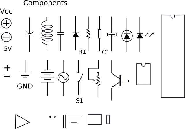
Inductors are represented by a series of loops or coils and are commonly used in power regulation, RF circuits, and noise suppression applications. Although inductors are generally fewer in number than resistors and capacitors, they often play a disproportionate role in maintaining power integrity. A clear schematic representation helps ensure that the correct inductance value, current rating, and package type are selected during sourcing and assembly.
| Symbol | Component | Function |
|---|---|---|
| Zigzag / box | Resistor (R) | - Limits current and sets bias points |
| Two parallel lines | Capacitor (C) | - Stores and releases electrical energy |
| Coil | Inductor (L) | - Stores energy in a magnetic field |
| Ferrite bead | Noise suppression | - Filters high-frequency interference |
Active components require an external power source and are responsible for signal control, amplification, and logic processing. These components are typically more complex and highly sensitive to orientation and pin configuration.
Diodes are represented by a triangle pointing toward a line, visually indicating the permitted direction of current flow. LED symbols include additional arrows to represent light emission. Incorrect diode orientation is a frequent cause of non-functional boards, particularly in early-stage designs. Clear polarity indicators within schematic symbols significantly reduce this risk during automated assembly.
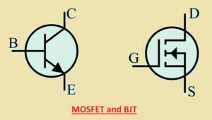
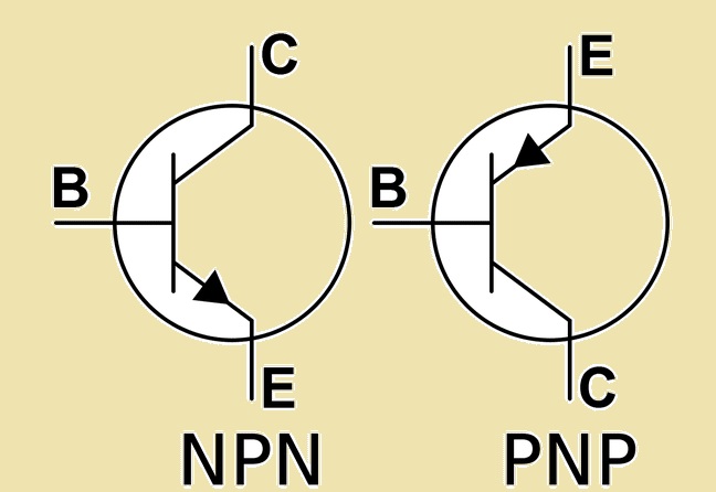
Transistor symbols—covering BJTs, MOSFETs, and related devices—use multi-terminal representations that define emitter, base, collector, or gate, drain, and source connections. These symbols convey critical information about switching behavior, signal direction, and biasing requirements.
Because transistors are often used in power regulation and signal control roles, inaccurate schematic representation can lead to overheating, inefficiency, or complete circuit failure. PCB manufacturers rely on precise transistor symbols and annotations to confirm footprint selection and assess thermal considerations during design review.
Integrated circuits are typically represented as rectangular symbols with clearly labeled pins for inputs, outputs, power, and ground. Modern PCBs may contain dozens—or even hundreds—of ICs, many packaged in fine-pitch surface-mount formats.
Accurate IC symbols ensure correct pin mapping, reliable power distribution, and predictable signal routing. During PCBA, pin-1 orientation errors are among the most severe assembly mistakes, often rendering an entire board unusable. Clear schematic symbols are therefore essential for first-pass assembly success.
| Symbol | Component | Function |
|---|---|---|
| Triangle + line | Diode (D) | - Allows current in one direction |
| LED arrowed symbol | Light-Emitting Diode (LED) | - Emits light when current flows |
| Complex multi-terminal | Transistor (Q) | - Amplifies/switches signals |
| Rectangles with many pins | Integrated Circuit (U/IC) | - Logic, processing, control |
Power and ground symbols define how energy is distributed throughout a circuit. Common examples include VCC or VDD symbols for supply rails, multiple ground symbols for signal, chassis, or earth ground, and voltage source or battery symbols.
Power integrity issues are a leading cause of PCB malfunction, and many originate from poor schematic representation rather than layout defects. Clear and consistent power and ground symbols allow manufacturers to verify net connectivity and assess power distribution early in the production process.


Source: Adapted from "PCB Design Technology and Practice" (4th ed.), by Zhiwei Huang, 2024, Publishing House of Electronics Industry.
Organizing component symbols into clear categories provides tangible manufacturing benefits. It accelerates schematic reviews, reduces layout misinterpretation, improves BOM accuracy, and streamlines PCB assembly and inspection.
Engineering workflows at professional PCB service providers benefit directly from this clarity, enabling faster turnaround times and fewer clarification cycles—particularly for complex designs that combine surface-mount and through-hole technologies.
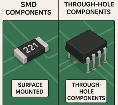
As electronic products continue to become smaller, faster, and more complex, PCB assembly methods have evolved to support higher component density and greater manufacturing efficiency. Although schematic symbols primarily represent electrical function, they also provide essential contextual information that influences whether a component is implemented using through-hole or surface-mount technology in the physical design.
Understanding how schematic symbols relate to mounting technologies is critical for accurate PCB design and reliable assembly outcomes.
Through-hole components are installed by inserting their leads through drilled holes in the PCB and soldering them on the opposite side. In schematic diagrams, through-hole components generally use the same electrical symbols as their surface-mount equivalents; the distinction lies in how those symbols are later mapped to physical footprints.
Through-hole technology is most commonly used for components that must handle higher power levels, provide mechanical strength, or support repeated mechanical stress. Typical applications include power components, connectors, and headers, as well as prototyping and educational designs where ease of handling and modification is important.
From a manufacturing standpoint, through-hole assembly introduces additional processing steps such as manual insertion or wave soldering, which can increase production time and cost. As a result, modern PCB designs tend to limit through-hole components to cases where they are functionally or mechanically necessary. PCB manufacturers support both through-hole and mixed-technology assembly, but clear schematic annotations help determine which components must remain through-hole and which can be converted to SMD for improved efficiency.
Surface-mount devices are soldered directly onto the surface of the PCB without the need for drilled holes. The vast majority of modern commercial electronics rely on SMD components due to their compact size, low weight, and compatibility with fully automated assembly processes.
Although schematic symbols for SMD components appear identical to those used for through-hole parts, the mounting method is defined through supporting design data such as footprint selection, reference designators, BOM descriptions, and assembly notes. Modern PCB designs frequently use extremely small SMD packages, such as 0402 or even 0201, where placement accuracy and orientation are critical. In these cases, even small ambiguities in the schematic can lead to costly assembly errors.
NextPCB’s PCBA processes are optimized for high-density SMD assembly, making precise symbol usage and correct symbol-to-footprint mapping essential for achieving high first-pass yield.
While schematic symbols alone do not explicitly indicate whether a component is through-hole or surface-mount, experienced designers and manufacturers infer the mounting method from associated documentation. This typically includes footprint library assignments, BOM package descriptions, and assembly drawings.
For example, a resistor symbol associated with a 0603 footprint clearly indicates an SMD component, while a capacitor symbol linked to a radial footprint denotes a through-hole part. Well-organized schematics and consistent labeling allow manufacturers such as NextPCB to quickly identify component types, optimize assembly workflows, and reduce delays caused by clarification requests.
Industry trends show that more than 90 percent of newly designed PCBs today rely primarily on SMD components. This dominance is driven by several key advantages, including higher component density, faster automated assembly, lower production costs at scale, and improved electrical performance due to shorter lead lengths.
However, these benefits also increase the importance of schematic accuracy. Smaller components provide less tolerance for placement and orientation errors, making precise symbol definition and documentation essential. NextPCB’s automated assembly lines and inspection systems are designed to manage these challenges, but overall manufacturing success still depends heavily on schematic quality.
Many real-world PCB designs combine both SMD and through-hole components to balance performance, cost, and mechanical requirements. These mixed-technology boards require particularly clear schematic documentation to prevent confusion during assembly.
Clear symbol usage and annotation support correct assembly sequencing, appropriate soldering method selection, and accurate cost estimation. This is an area where experienced PCB service providers such as NextPCB add significant value by reviewing designs to ensure that schematic intent aligns with manufacturing reality.
Beyond schematic symbols themselves, electronic schematics rely heavily on reference designators, labels, and value annotations to uniquely identify every component in a circuit. These identifiers are essential for translating a design from concept into fabrication, assembly, testing, and long-term maintenance. In PCB manufacturing, reference designators form the critical link between the schematic, the PCB layout, the bill of materials, and the fully assembled board. Without consistent and clearly defined labeling, even a well-engineered circuit can become difficult, or in some cases impossible, to manufacture correctly.
A reference designator is a standardized identifier consisting of a letter prefix followed by a number, used to uniquely distinguish each component in a design. The prefix indicates the component type, such as resistors, capacitors, inductors, diodes, transistors, integrated circuits, connectors, or test points, while the number differentiates individual instances of that component type. These conventions allow designers, assemblers, inspectors, and test technicians to refer to the same component unambiguously across all project documentation.
| Prefix | Component Type |
|---|---|
| R | Resistor |
| C | Capacitor |
| L | Inductor |
| D | Diode / LED |
| Q | Transistor |
| U / IC | Integrated Circuit |
| J | Connector |
| TP | Test Point |
In modern, high-density PCB designs—where hundreds or even thousands of components may be present—clear and consistent reference designators are especially important. They reduce ambiguity during placement and inspection and make it far easier to locate specific components during debugging or rework.
During PCB assembly, reference designators play a central operational role. They are used to match BOM entries to specific physical locations on the board, program pick-and-place machines, verify correct placement during optical or X-ray inspection, and identify components during troubleshooting and repair. Assembly experience across the electronics industry shows that duplicated, missing, or inconsistent reference designators are a frequent cause of production delays, often resulting in clarification requests or temporary manufacturing holds. NextPCB depends on clean, well-organized reference designators to maintain efficient automation and fast assembly turnaround, particularly for high-volume or high-density SMD boards.
In addition to reference designators, schematic symbols are annotated with component values and key electrical characteristics. These annotations typically include resistance, capacitance, voltage rating, power rating, and tolerance, depending on the component type. For polarized components, polarity markings or orientation notes are equally important, as they directly affect assembly correctness and circuit functionality.
Even when a symbol is electrically correct, missing or ambiguous value annotations can lead to incorrect component sourcing, substitution errors, or performance issues. To prevent this, NextPCB verifies that schematic annotations align precisely with BOM specifications before production begins.
Integrated circuits require more detailed labeling than most passive components. In addition to reference designators, IC symbols often include part numbers, functional pin names, and clearly identified power and ground connections. Orientation markers, such as pin-1 indicators, are also critical, particularly for surface-mount packages with fine pitch leads. Because many ICs are available in multiple package types and pin configurations, accurate labeling ensures that the correct footprint is selected and that orientation during assembly is correct. This level of precision is especially important in automated SMD assembly, where even a single orientation error can render an entire PCB unusable.
Reference designators and labeling continue to provide value long after manufacturing is complete. They simplify troubleshooting during testing, support efficient repairs in the field, and make future redesigns or upgrades significantly easier. Well-labeled schematics improve overall documentation quality and ensure that design intent remains clear even years after the original development effort. For professional electronics development, this traceability is not optional—it is a foundational requirement for scalable, maintainable products. 4.
Understanding electronic component symbols is only the starting point. The real challenge in PCB development lies in ensuring those symbols are interpreted correctly and implemented accurately throughout fabrication and assembly. This transition, from schematic representation to physical PCB, is where many otherwise sound designs encounter problems, not because the concept is flawed, but because design intent is lost or misinterpreted during manufacturing. This is where NextPCB provides measurable and practical value.

Once a schematic is finalized, it becomes the authoritative reference for PCB layout, footprint assignment, component sourcing, assembly programming, and quality inspection. Any ambiguity or inconsistency at this stage can propagate downstream, increasing the likelihood of errors.
NextPCB’s workflow is designed to preserve schematic intent across every production step. By reviewing schematics, PCB layout files, and BOMs together as a unified design package,
NextPCB engineers can identify and resolve issues such as symbol-to-footprint mismatches, incorrect polarity or orientation definitions, missing or unclear component values, and inconsistent reference designators. Detecting these issues early significantly reduces the risk of rework and improves first-pass manufacturing yield.
Contemporary PCBs rarely rely on a single component type or mounting technology. Most designs incorporate a mix of passive components in various SMD sizes, active devices in fine-pitch packages, and power components or connectors that require mechanical robustness.
NextPCB supports surface-mount, through-hole, and mixed-technology assemblies, with engineering expertise that aligns closely with standard component symbol classifications. This familiarity allows their engineers to understand not only what a schematic symbol represents electrically, but also how the corresponding component behaves during real-world assembly and soldering processes. As a result, potential manufacturing concerns can be addressed before production begins.
Rather than treating design for manufacturability (DFM) as an optional or late-stage activity, NextPCB integrates DFM checks into its standard workflow. This includes verifying that schematic symbols accurately reflect component behavior, confirming that selected footprints match package specifications, ensuring polarized components are clearly defined, and validating that power and ground symbols align with layout connectivity.
Industry experience consistently shows that early DFM-driven reviews can reduce total project costs by up to 30 percent by preventing late-stage corrections and board respins. NextPCB’s approach reflects this reality, enabling designers to move from schematic to production with greater confidence and fewer surprises.
Clear schematics and accurate symbol implementation are especially important in global manufacturing environments. NextPCB’s online ordering system, combined with professional engineering review, allows designs to progress from upload to fabrication and assembly with minimal clarification cycles, regardless of customer location.
This efficiency is reinforced by NextPCB’s streamlined logistics model, which supports fast and reliable global shipping, minimizing delays between design completion and product delivery.
For designers and engineers, accurate symbol implementation results in fewer design revisions, faster production timelines, and greater confidence in the final hardware. For manufacturers, it provides clear instructions, reduces assembly errors, and improves yield consistency and overall quality. By aligning schematic clarity with disciplined manufacturing execution, NextPCB ensures that electronic component symbols are not merely understood in theory but faithfully realized in physical form.

China's Biggest Electronics Components Distributor
Mastering electronic component symbols goes far beyond memorization. To produce PCBs that are electrically correct, manufacturable, and reliable, designers must apply consistent best practices that reduce ambiguity and strengthen communication between design and manufacturing teams.
Designers should rely on trusted symbol libraries that conform to recognized standards such as IEC or ANSI. Standardized symbols reduce interpretation errors and ensure consistency across schematic, layout, and assembly documentation. Custom symbols should be avoided unless necessary, as nonstandard representations increase the likelihood of misunderstanding during layout review and PCBA.
It is also essential to verify that each symbol accurately reflects the intended component behavior, including polarity, pin assignments, and functional characteristics. Many modern PCB design tools include validated symbol libraries that align well with NextPCB’s design-for-manufacturability checks, helping minimize fabrication and assembly issues.
Every schematic symbol should include a unique reference designator and complete value annotation. This includes component values, tolerances, voltage or power ratings, and polarity indicators where applicable. For integrated circuits and other multi-pin devices, pin-1 orientation and power or ground pins must be clearly identified.
Clear annotation directly reduces assembly and inspection errors and significantly simplifies debugging—especially on dense SMD boards where visual identification is more challenging.
A frequent source of manufacturing errors is misalignment between schematic symbols, PCB footprints, and BOM entries. Designers should confirm that each symbol maps to the correct package type and footprint and that BOM information matches the symbol in part number, value, and orientation.
Extra care is required for fine-pitch SMD components such as 0402 and 0201 packages, where placement or polarity errors are difficult and costly to correct. NextPCB’s engineering review process includes systematic cross-checks between schematics, footprints, and BOMs to prevent these issues before production begins.
Before transitioning to PCB layout, designers should validate circuit functionality using simulation tools and conduct structured schematic reviews. Peer reviews or formal engineering checks often uncover issues related to connectivity, orientation, or labeling that might otherwise reach the assembly stage.
Considering manufacturability early—such as component accessibility for soldering and testing—further reduces risk. Industry data shows that early validation can reduce first-pass assembly failures by more than 20 percent.
Readable schematics are easier to manufacture. Designers should use consistent line styles, spacing, and annotation placement throughout the schematic, and include legends for any uncommon or specialized symbols. All diagrams should remain legible at standard PDF or print scale without requiring excessive zooming.
Clean, standardized documentation allows manufacturers like NextPCB to interpret designs quickly, reduce clarification cycles, and accelerate assembly timelines.
Engaging PCB manufacturers early in the design process provides valuable insight into symbol clarity, footprint compatibility, and manufacturability concerns. Experienced partners such as NextPCB can identify symbol-related risks that may affect assembly, inspection, or long-term reliability.
This collaboration reduces uncertainty, shortens production cycles, and improves overall product quality.
Even with a foundational understanding of electronic component symbols, beginners frequently make mistakes that undermine PCB functionality, manufacturability, and assembly yield. Identifying these issues early helps prevent rework, reduce delays, and ensure a smoother transition from schematic to finished PCB.
One of the most common beginner errors involves incorrect polarity or orientation of components such as diodes, LEDs, electrolytic capacitors, and integrated circuits. These components depend on precise directional placement to function correctly.
The impact can be immediate and severe, ranging from non-functional circuits to short circuits and permanent component damage. Industry data indicates that more than 25 percent of PCB assembly errors stem from polarity and orientation mistakes, particularly in surface-mount designs.
To mitigate this risk, designers should carefully verify symbol polarity markers, pin-1 indicators, and schematic annotations. Using manufacturer-verified footprints further reduces ambiguity. Professional PCBA services, such as NextPCB, include polarity verification during assembly preparation to catch these issues before soldering begins.
Beginners may also misinterpret visually similar symbols, such as confusing resistors with inductors in dense schematics, mislabeling voltage sources, or misunderstanding transistor and IC pin configurations.
These errors can lead to signal degradation, unstable operation, or damage to high-value components. The best defense is consistent use of standardized symbol libraries and clear schematic labeling. Well-organized schematics make functional intent easier to understand during both layout and assembly.
Another frequent issue is inconsistent or missing reference designators, along with misalignment between schematic symbols and the bill of materials. Duplicate designators or mismatched BOM entries can confuse assembly teams and automated pick-and-place systems.
Manufacturing reports indicate that BOM-related inconsistencies contribute to as much as 15 percent of first-pass failures in new PCB designs. Working with experienced manufacturers like NextPCB helps prevent these problems, as their engineering teams systematically cross-check schematics, footprints, and BOMs before production.
Beginners often focus solely on electrical correctness while overlooking manufacturability. Ignoring component spacing, footprint accessibility, soldering constraints, or inspection requirements can lead to costly redesigns and extended production timelines.
Conducting DFM reviews before fabrication is essential. NextPCB provides DFM guidance that ensures schematic symbols, footprints, and layouts translate efficiently into manufacturable, high-yield PCBs.
Small surface-mount components require far greater placement accuracy than through-hole parts. Beginners sometimes treat them interchangeably, failing to account for pad geometry, thermal balance, or orientation sensitivity.
This oversight can result in tombstoning or misplacement—issues that occur in up to 8 percent of early production runs for high-density SMD boards. NextPCB’s automated SMD assembly processes, combined with careful schematic and footprint review, significantly reduce these risks.
1) What are electronic component symbols?
Electronic component symbols are standardized graphical representations of electrical and electronic components in a schematic. They communicate the function, polarity, connectivity, and type of each component without showing its physical appearance. Using standardized symbols ensures clarity for both PCB designers and manufacturers.
2) Why are symbols important in PCB design?
Symbols act as a bridge between schematic design and real PCB assembly. Accurate symbols reduce errors, ensure correct component placement, and support efficient manufacturing, especially for high-density SMD boards. Manufacturers like NextPCB rely on clear symbols to verify designs and improve first-pass yield.
3) What is the difference between through-hole and SMD symbols?
Through-hole symbols are used for components with leads that go through drilled PCB holes.
SMD symbols represent components mounted directly on the PCB surface.
Although the symbols may look similar, the footprints and assembly methods differ, so careful annotation and BOM alignment are essential for manufacturing.
4) What are reference designators, and why are they important?
Reference designators (like R1 for resistors, C2 for capacitors, U1 for ICs) uniquely identify each component in a schematic. They are crucial for:
Correct BOM creation
Automated pick-and-place assembly
Troubleshooting and maintenance
Clear reference designators help manufacturers like NextPCB assemble boards efficiently and accurately.
5) How do symbols affect component orientation and polarity?
Symbols often indicate polarity or direction for diodes, LEDs, polarized capacitors, and ICs. Misinterpreting these symbols can lead to non-functional boards or component damage. Manufacturers like NextPCB include polarity verification in their assembly process to prevent these errors.
6) Can I use custom symbols in schematics?
Yes, but only when necessary. Nonstandard symbols increase the risk of misinterpretation and may slow down manufacturing or cause errors. It’s best to use verified, standardized libraries and cross-check them with BOMs and footprints.
7) How does NextPCB help with schematic symbols?
NextPCB supports designers by:
Reviewing schematic symbols for accuracy
Cross-checking symbols with footprints and BOM
Providing DFM guidance for manufacturability
Ensuring correct SMD and through-hole assembly
This reduces errors, speeds up production, and ensures that the final PCB matches the design intent.
8) What are the most common mistakes beginners make with symbols?
Misinterpreting polarity or orientation
Confusing similar symbols
Ignoring reference designators or BOM alignment
Overlooking DFM considerations
Failing to differentiate between SMD and through-hole components
Avoiding these mistakes improves design reliability and reduces costly rework.
9) Where can I learn to read electronic component symbols?
Use online tutorials and PCB design software libraries
Refer to NextPCB blogs on component identification and PCBA guides
Study standardized references such as IEC/ANSI standards
Hands-on practice with schematics and PCB layouts is also highly recommended.
10) Are electronic component symbols the same worldwide?
Mostly yes. International standards like IEC and ANSI ensure that symbols are consistent across regions and tools. This standardization allows global collaboration between designers and manufacturers, which is crucial for companies like NextPCB that serve international clients.
Electronic component symbols are more than schematic illustrations—they are the universal language connecting design intent to real-world PCB manufacturing. From passive components like resistors and capacitors to complex ICs and power networks, each symbol carries critical information that affects layout, assembly accuracy, and overall product reliability. In modern electronics, where over 90% of PCBs rely on surface-mount components, even small errors in symbol clarity or annotation can result in costly orientation or polarity mistakes, as well as BOM inconsistencies that contribute to first-pass failures.
Proper application of symbols ensures that designs are accurate, manufacturable, and reliable. Correct symbols improve component placement, reduce rework and scrap, lower production costs, and accelerate time-to-market. Mastering symbols is therefore not just an academic exercise—it is a professional skill that bridges schematic intent and production reality. Designers who pair precise schematics with expert manufacturing support gain a significant advantage in delivering functional, high-quality PCBs on schedule.
NextPCB provides the solution for turning schematic precision into manufacturing success. Through comprehensive schematic verification, BOM cross-checking, and design-for-manufacturability (DFM) reviews, along with advanced SMD and through-hole assembly capabilities, NextPCB ensures that every symbol is accurately translated into a physical board. Combined with fast-turn production and global logistics support, this approach transforms abstract schematics into reliable, high-performing PCBs—allowing designers to move from concept to finished hardware with confidence and efficiency.
Get BOM Services Engineer Consultation
>> About the Author
Abiola Ayodele: Broadcast Journalist & Tech Writer; Cooperate writer of NextPCB.
Specialize in technical writing, and editing, particularly in the areas of PCB design, semiconductors, cybersecurity, and emerging engineering technologies.
Still, need help? Contact Us: support@nextpcb.com
Need a PCB or PCBA quote? Quote now


 Surface