
 NextPCB Capabilities
Printed Circuit Boards
NextPCB Capabilities
Printed Circuit Boards
 PCB Assembly
 Layer Buildup
 SMD-Stencils
 PCB Design-Aid & Layout
 Mechanics
 Quality
 Drills & Throughplating
 Factory & Certificate
 PCB Assembly Factory Show
Certificate
PCB Assembly Factory Show
Certificate
Support Team
Feedback:
support@nextpcb.com


Capacitor symbols act as the universal language bridging early-stage circuit design and physical PCB manufacturing. As electronic devices shrink and High-Density Interconnect (HDI) boards become the industry standard, these symbols do much more than represent basic energy storage. They communicate critical engineering parameters—such as polarity, variability, package sizing, and capacitor type—directly to layout engineers, procurement teams, and assembly technicians.
When executing a schematic capture, the symbol you select must dynamically link to a specific physical footprint and 3D step model. A mismatch at this stage—such as using a non-polarized symbol for a polarized tantalum capacitor, or associating an 0805 footprint with an 0402 schematic symbol—can bypass standard Design Rule Checks (DRC). During the PCBA reflow process, this leads to tombstoning, reverse-bias explosions, or components simply not fitting on the board. Standardized, data-rich symbols ensure that from initial SPICE simulation to final turnkey PCB assembly, every stakeholder interprets the Bill of Materials (BOM) intent with zero ambiguity.
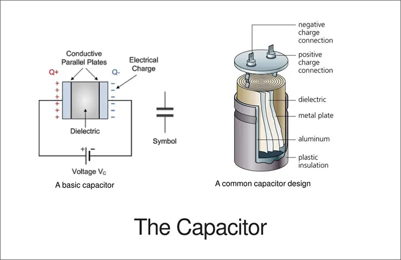
At its core, the most fundamental electronic symbol for capacitor consists of two parallel lines separated by a gap, representing the physical conductive plates and the insulating dielectric. While this basic representation confirms the presence of capacitance in a circuit, it lacks specific Design for Manufacturing (DFM) data.
Modern hardware developers must attach rich metadata to these symbols. Parameters such as voltage rating, capacitance tolerance, equivalent series resistance (ESR), and dielectric material (e.g., C0G, X7R, Y5V) dictate the physical realities of the component. For example, a 10uF ceramic capacitor requires a vastly different footprint depending on whether it is rated for a 10V low-power IoT device or a 100V industrial power supply.
Below is a technical reference mapping physical capacitor types to their standard schematic symbols, bridging the gap between schematic capture and the physical assembly line.
| Physical Component | Schematic Symbol | Capacitor Type |
|---|---|---|
 |
 |
Disc Ceramic Capacitor |
 |
 |
Multilayer Ceramic Capacitor (MLCC) |
 |
 |
Metalized Film Capacitor |
 |
 |
Mica Capacitor |
 |
 |
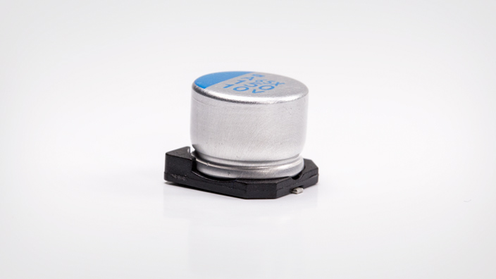
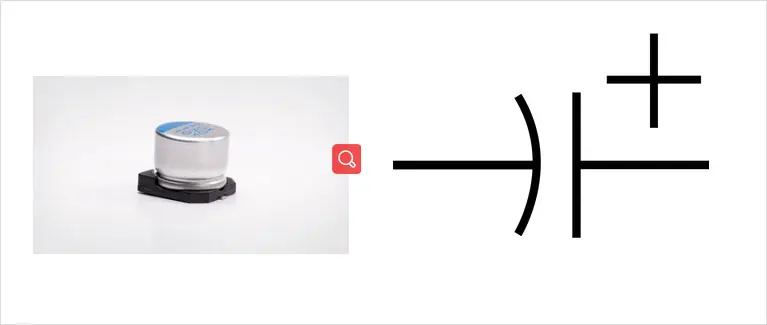
Aluminum Electrolytic Capacitor |
 |
 |
Tantalum Electrolytic capacitor |
 |
 |
Niobium Electrolytic Capacitor |
 |
 |
Aluminum Polymer Capacitor |
 |
 |
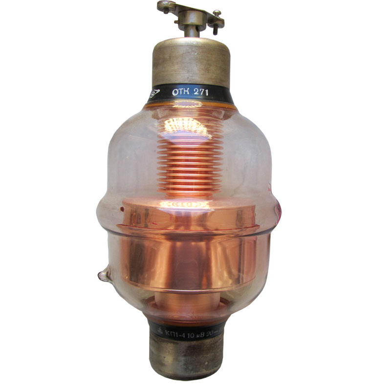
Variable Vacuum Capacitor |
 |
 |
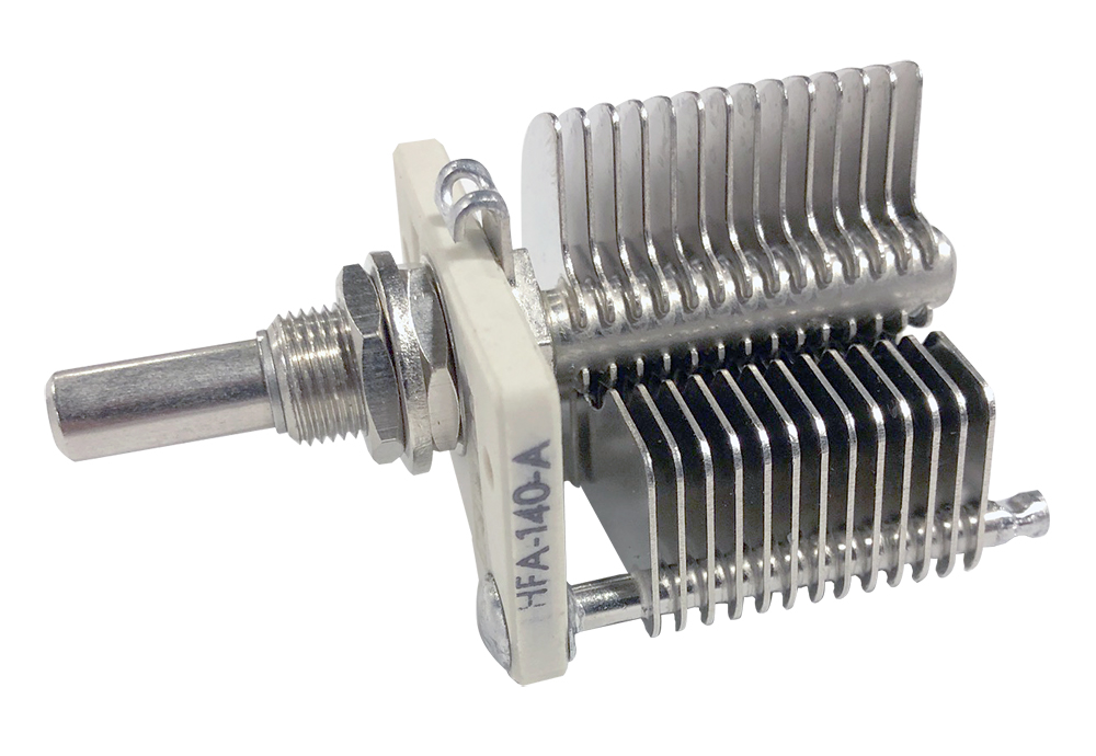
Variable Air Gap Capacitor |
 |
 |
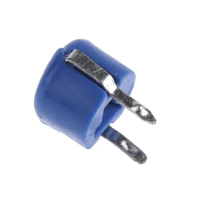
Ceramic Trimmer Capacitor |
 |
 |
Film Trimmer Capacitor |
 |
 |
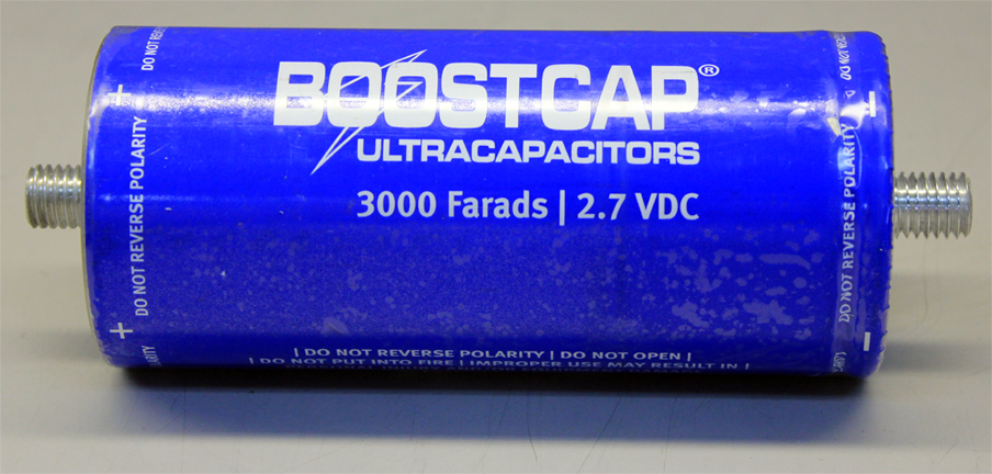
Supercapacitor |
 |
 |
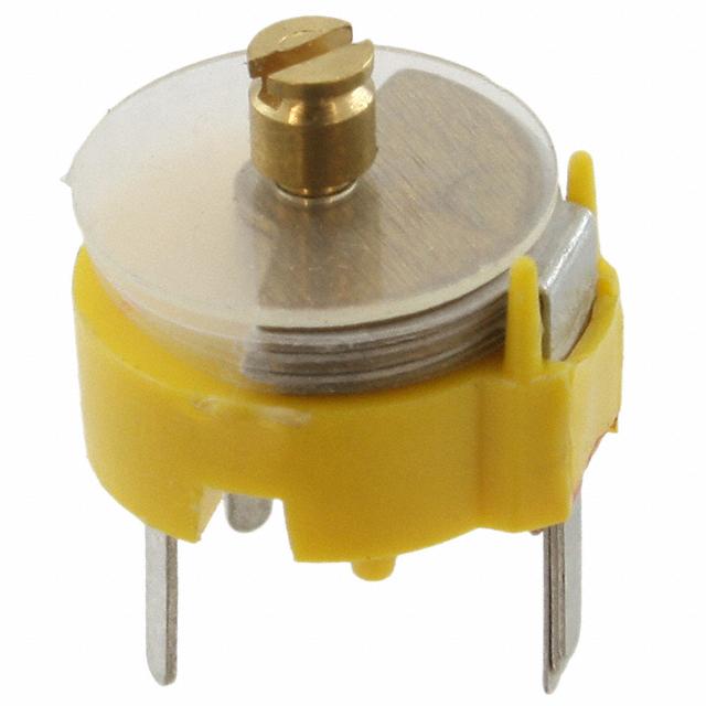
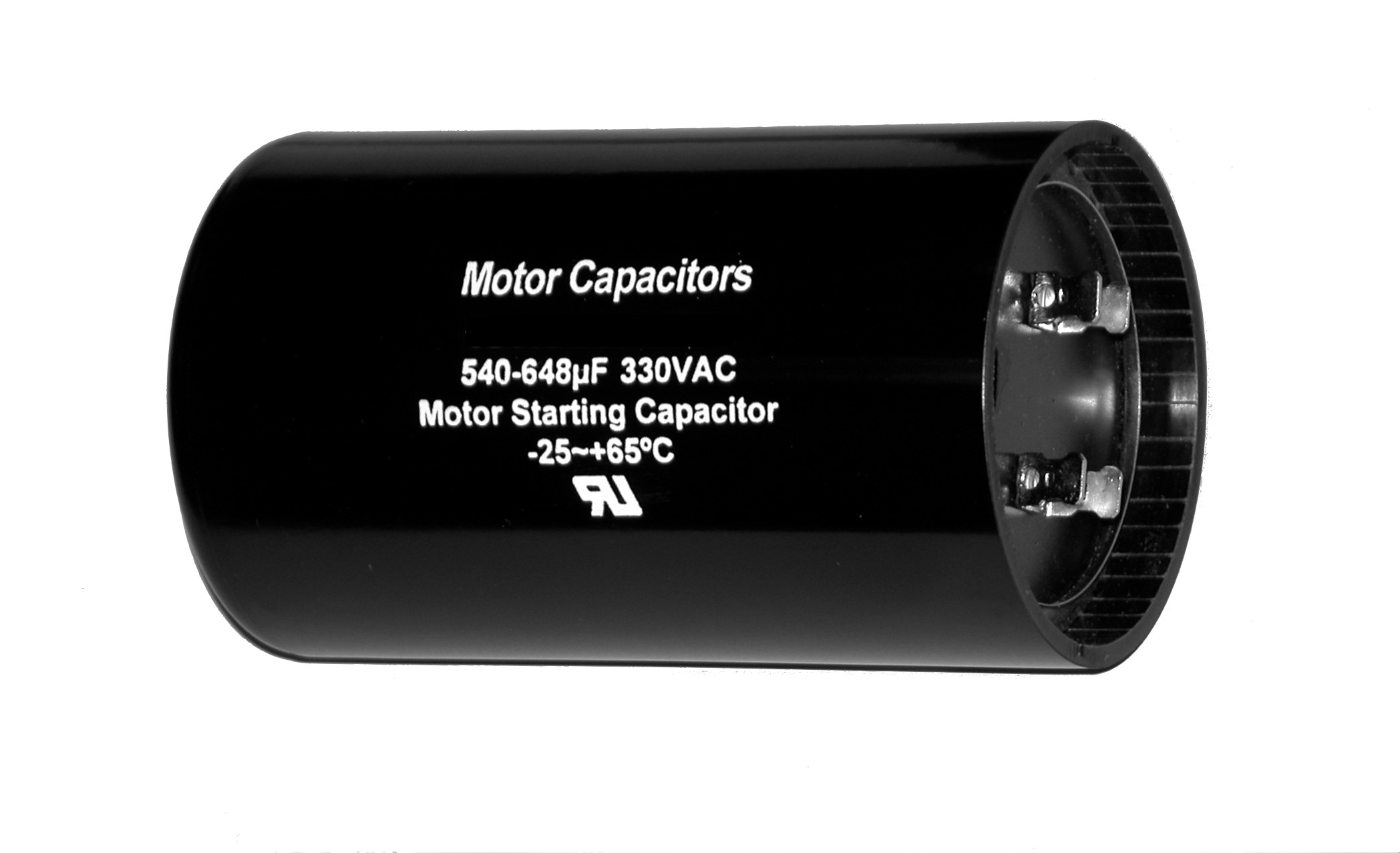
Motor Run and Start Capacitor |
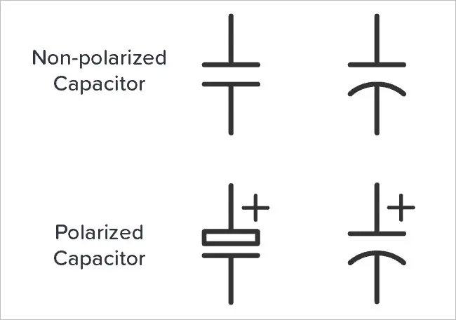
A fixed capacitor maintains a constant capacitance value. In schematics, these utilize the standard non-polarized symbols (two parallel lines). Hardware engineers frequently deploy them for high-frequency decoupling, signal filtering, and DC blocking across various PCB substrates.
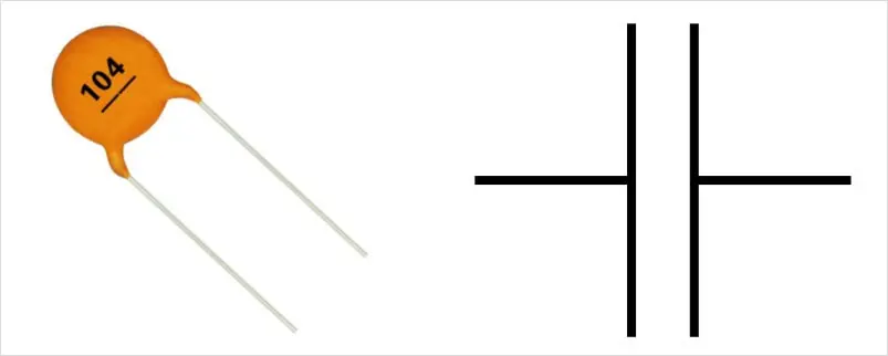
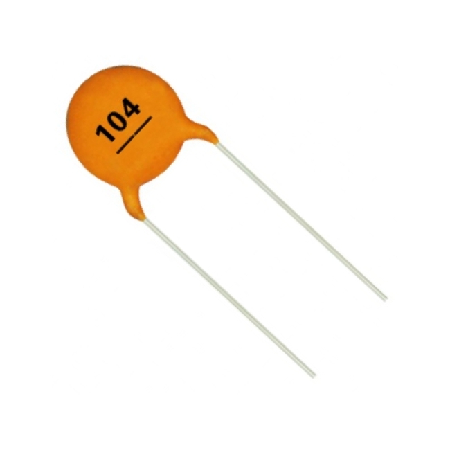
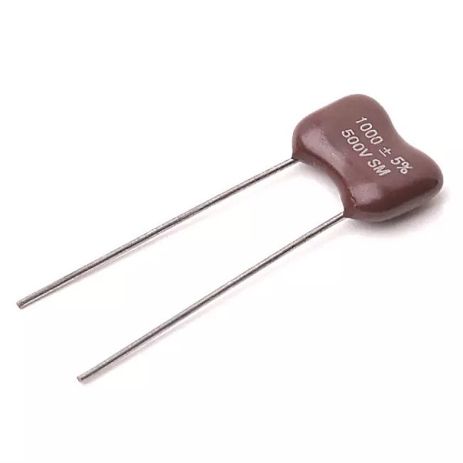
Disc Ceramic Capacitors: Formed from a ceramic disc coated with silver electrodes, these through-hole components excel in high-voltage applications. Due to their higher parasitic inductance, they are less ideal for high-speed digital designs but perfect for bulk power supply filtering on standard FR4 PCB manufacturing runs.
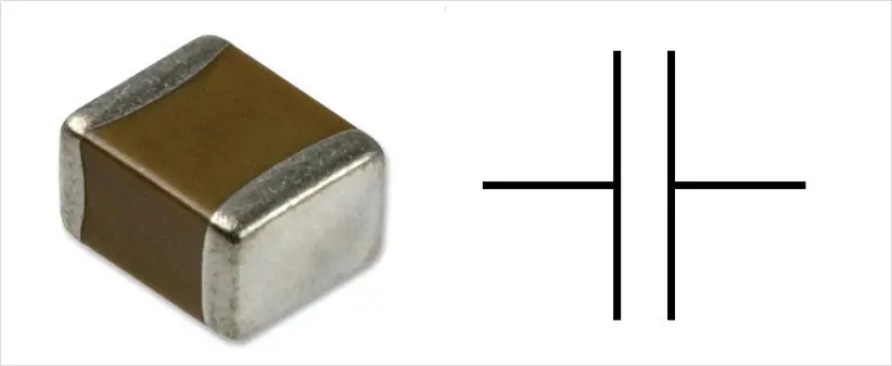
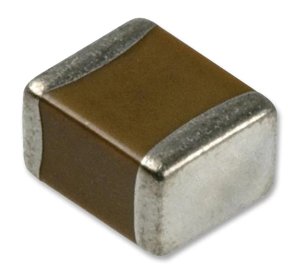
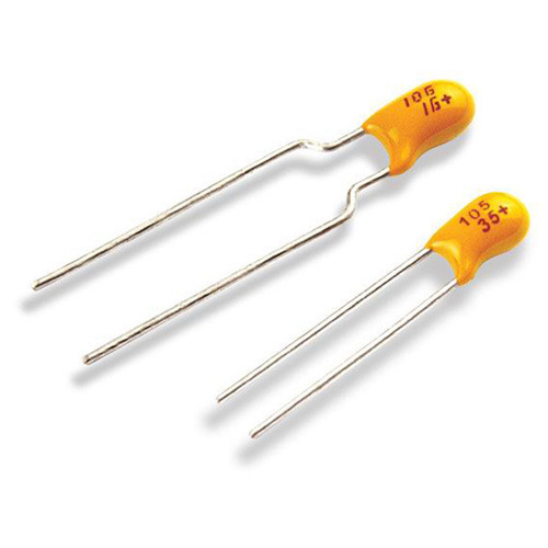
Multilayer Ceramic Capacitors (MLCC): The undisputed backbone of modern PCBA. MLCCs stack alternating layers of ceramic dielectric and metal electrodes. Because they exhibit exceptionally low Equivalent Series Resistance (ESR) and Equivalent Series Inductance (ESL), layout engineers place them as close to IC power pins as possible for high-speed decoupling. When submitting Gerbers for a low cost PCB, standardizing your MLCC footprint sizes (e.g., relying on standard 0402 or 0603 rather than pushing for ultra-micro 01005 unless necessary) helps optimize BOM cost, reduces bare board complexity, and accelerates pick-and-place assembly.
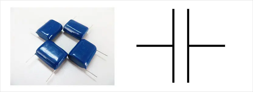
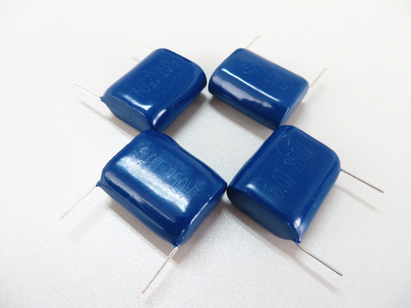
Film capacitors utilize thin plastic or polymer films (polyester, polypropylene, PTFE) as the dielectric. They are highly stable over extreme temperature variations and resist aging far better than ceramics. You will commonly find these in audio crossover networks, automotive EV circuits, and high-current power inverters. Metalized Film Capacitors have the added advantage of "self-healing"—localized dielectric breakdowns simply vaporize the tiny metal coating around the fault, preventing a catastrophic dead short and preserving system uptime.
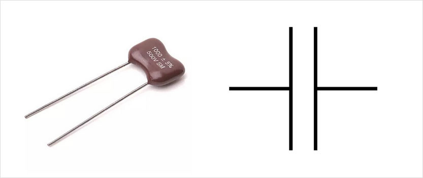
For RF engineering and critical timing circuits, Mica and Glass capacitors provide unmatched precision and lowest possible signal loss. When designing advanced high-frequency boards operating in the gigahertz or sub-THz ranges (such as 110GHz+ R&D testing environments), pairing advanced substrates like Rogers, PTFE, or ceramic with high-Q mica capacitors minimizes signal distortion. The schematic symbol remains the standard parallel lines, but the DFM parameters must explicitly state the tight tolerance requirements to ensure the factory procures the exact part.
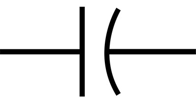
Polarized symbols demand absolute attention during the layout and routing phase. Connecting these components backward results in out-gassing, swelling, and violent ruptures during operation or immediate failure during functional testing.
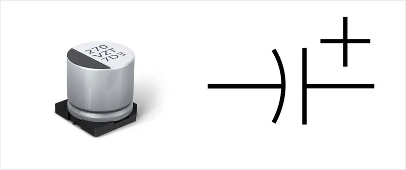
An Aluminum Electrolytic Capacitor uses an anodized aluminum foil as the positive plate (anode) and a liquid or gel electrolyte as the cathode. They offer massive capacitance values necessary for smoothing rectified DC voltages. In schematic capture, always use the polarized symbol (straight line for positive, curved or hashed line for negative). Crucially, ensure your PCB layout silkscreen clearly marks the positive pad and footprint orientation to comply with IPC-A-600 quality standards and guide the assembly machines.
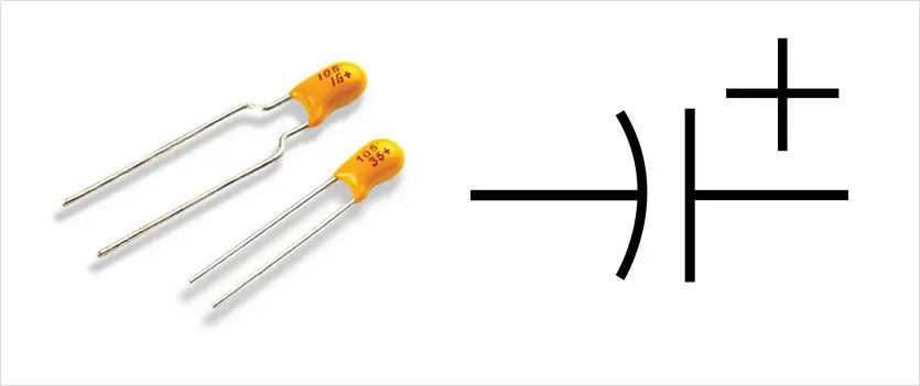
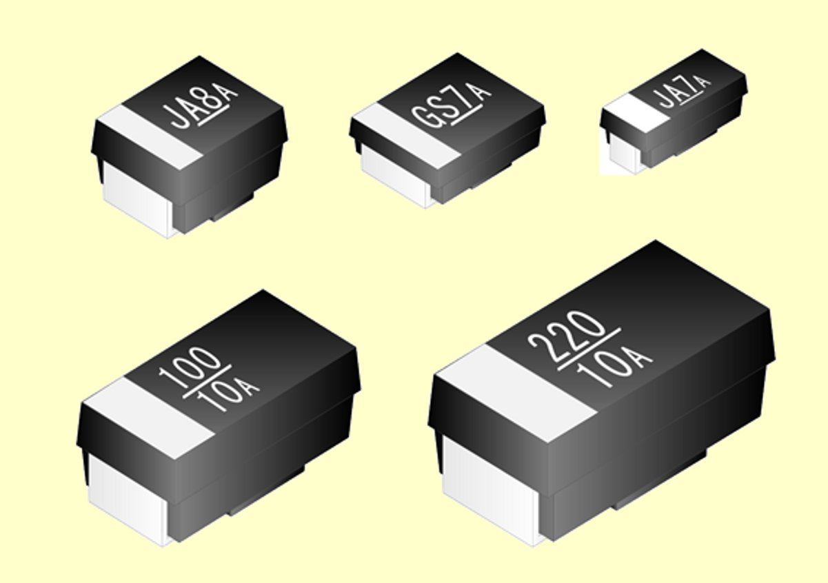
Tantalums provide superior capacitance density and lower ESR than standard aluminum types, packaged in highly compact SMD form factors perfect for densely packed boards. However, they are famously unforgiving to reverse voltage and inrush current spikes. A robust DFM check must ensure the polarized schematic symbol aligns perfectly with the layout footprint polarity indicator, as a backward tantalum will reliably catch fire on the test bench.
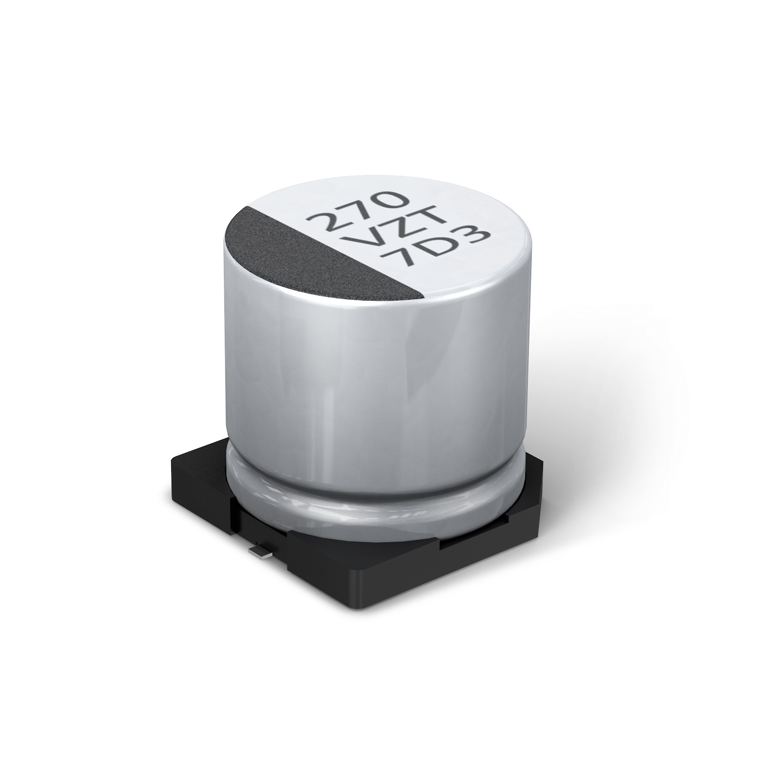
To combat the ignition risks of tantalum and the drying-out phenomenon of liquid aluminum capacitors, engineers increasingly specify Niobium and Aluminum Polymer Capacitors. Polymer capacitors replace the liquid electrolyte with a highly conductive solid polymer. They easily handle the aggressive thermal profiles of lead-free PCBA reflow ovens without performance degradation or bulging over time.
When a circuit requires active tuning—such as matching antenna impedance, calibrating a crystal oscillator, or adjusting a high-frequency filter—variable capacitors are utilized. A diagonal arrow striking through the parallel plates generally denotes this variability in schematic design.
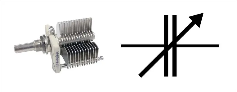
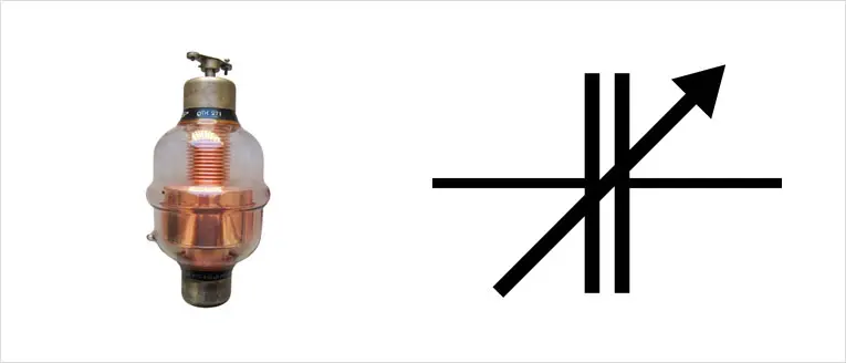
Air Gap Capacitors mesh a set of stationary plates (stator) with rotating plates (rotor), changing capacitance via mechanical adjustment. Vacuum Capacitors enclose the plates in a high-vacuum glass or ceramic envelope. This vacuum grants them extreme high-voltage ratings, making them a staple for heavy-duty RF transmitters, medical MRI machines, and industrial induction heating equipment.
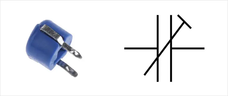
Unlike main variable capacitors intended for regular user adjustment, trimmers allow test engineers and technicians to calibrate the PCB during the final stages of manufacturing. The symbol features a T-shaped line ending on one of the parallel plates. DFM Check: Always ensure your 3D layout clearances accommodate a tuning screwdriver without risking shorts to adjacent active components.
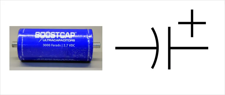
Supercapacitors provide massive energy density, utilized heavily for real-time clock (RTC) battery backups, IoT sensor arrays, and power-loss protection circuits. The schematic symbol often features a wider gap or a polarized marking. When integrating supercapacitors into a quick turn PCB, layout engineers must account for their physically large mechanical footprints and design circuitry to handle their incredibly high initial inrush current during the charging phase.
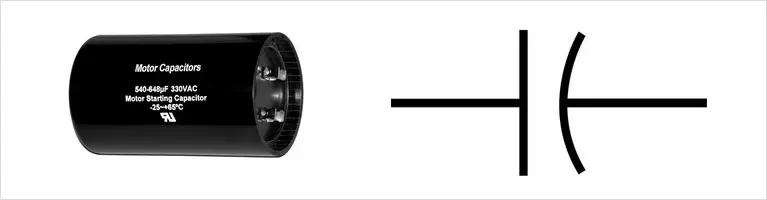
Used primarily in industrial power electronics, these rugged, non-polarized film or electrolytic capacitors handle continuous high-AC voltages to maintain motor phase shifts. They rarely appear on standard logic boards but are common in heavy-duty controller schematics.
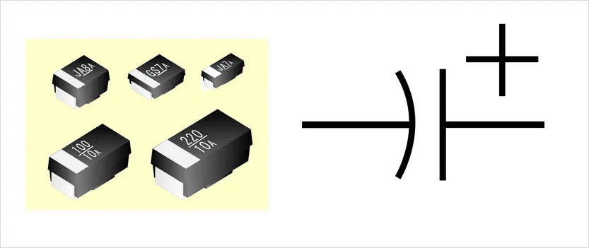
While the schematic symbols for a 10uF through-hole (THT) electrolytic and a 10uF surface-mount (SMD) electrolytic look identical on a digital schematic, the physical layout and assembly strategies are entirely different.
In modern EDA tools, your capacitor draw process must explicitly link the generic symbol to the precise footprint library (e.g., EIA 0805, 1206, or specific EIA 3216 tantalum case sizes). Failing to match the footprint to the exact manufacturer part number guarantees assembly line stoppages.
Global engineering teams utilizing outsourced manufacturing must recognize that a symbol for a capacitor can visually differ depending on the geographical origin of the schematic drafting standard.
Moving seamlessly from a theoretical schematic capture to a functional, physical board requires applying strict Design for Manufacturing (DFM) rules:
Transitioning from a prototype schematic to a mass production run? NextPCB offers seamless CAD-to-CAM translation and comprehensive engineering support.
Whether you need a rapid, low cost PCB run for R&D testing or high-volume turnkey PCB assembly, our DFM engineering team meticulously reviews your Gerbers, drill files, and BOM. We ensure your capacitor footprints match reality, preventing costly respins and ensuring rapid market delivery.
Start your project with NextPCB's smart quoting engine today.
The standard electronic symbol for a capacitor consists of two parallel lines separated by a gap. This gap visually represents the dielectric insulator placed between two conductive plates.
You can identify a polarized capacitor by looking for asymmetrical line structures in the symbol and explicit text markings that dictate installation orientation.
While the visual core of the capacitor symbol remains standardized, the workflow for executing a capacitor draw depends entirely on how the specific EDA software manages component libraries.
A generic schematic symbol simply indicates "capacitance," but it does not tell the manufacturer what physical material, size, or voltage rating to source for the automated PCBA process.
Selecting SMD capacitors for your design?

Arya Li, Project Manager at NextPCB.com
With extensive experience in manufacturing and international client management, Arya has guided factory visits for over 200 overseas clients, providing bilingual (English & Chinese) presentations on production processes, quality control systems, and advanced manufacturing capabilities. Her deep understanding of both the factory side and client requirements allows her to deliver professional, reliable PCB solutions efficiently. Detail-oriented and service-driven, Arya is committed to being a trusted partner for clients and showcasing the strength and expertise of the factory in the global PCB and PCBA market.
Still, need help? Contact Us: support@nextpcb.com
Need a PCB or PCBA quote? Quote now


 Surface

