NextPCB Capabilities
 PCB Assembly
 Layer Buildup
 SMD-Stencils
 PCB Design-Aid & Layout
 Mechanics
 Quality
 Drills & Throughplating
 Factory & Certificate





A transistor only amplifies cleanly when it is biased correctly and analyzed with the right small-signal model. This guide is a companion to our Electronic Devices and Circuits overview, and goes deep into BJT and FET biasing techniques, h-parameter small-signal analysis, transconductance, and the practical PCB layout decisions that determine whether an amplifier stage actually performs the way its schematic predicts.
1. Why Biasing and Small-Signal Analysis Matter
A transistor amplifier does two jobs at once: a DC biasing network sets a fixed operating point (the Q-point), and the AC signal rides on top of that DC point without disturbing it. Get the biasing wrong, and the output clips even if the AC gain calculation is perfect on paper. Small-signal analysis — using h-parameters for a BJT or a transconductance model for a FET — is how designers predict gain, input impedance, and output impedance for the AC signal once the DC operating point is fixed.
2. BJT Biasing Techniques in Detail
Fixed Bias
A single resistor from the supply to the base sets a fixed base current, IB = (VCC − VBE) / RB. It is the simplest circuit to design, but the operating point depends directly on the transistor’s current gain (β), which varies significantly between individual transistors and drifts with temperature — making this scheme unreliable for production designs.
Collector-to-Base (Collector-Feedback) Bias
Moving the base resistor from the supply to the collector introduces negative feedback: if collector current rises, collector voltage falls, which reduces base current and pulls collector current back down. This improves stability over fixed bias without adding components, though it also slightly reduces voltage gain due to the same feedback action.
Voltage-Divider (Self) Bias
A resistor divider (R1, R2) sets a fixed base voltage, and an emitter resistor (RE) provides additional stabilization: if collector current increases, emitter voltage rises, which reduces the effective base-emitter voltage and pulls the current back down. When the divider current is set well above the base current, the base voltage becomes almost independent of β, which is why this is the standard biasing scheme in production amplifier designs.
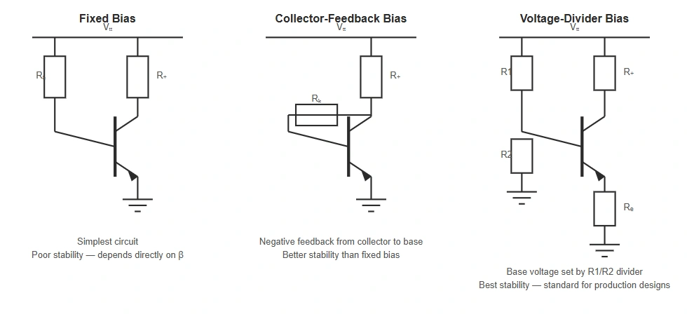
Bias Stability Compared
| Biasing Scheme | Component Count | Stability Against β Variation | Typical Use |
|---|---|---|---|
| Fixed bias | Lowest | Poor | Simple switching, non-critical circuits |
| Collector-to-base bias | Low | Moderate | Low-cost designs needing better stability than fixed bias |
| Voltage-divider bias | Highest | Best | Production amplifier stages |
3. BJT Small-Signal Analysis: h-Parameters
Once the DC operating point is set, the transistor’s AC behavior around that point is modeled with four hybrid (h) parameters: hie (input impedance), hre (reverse voltage feedback ratio, usually small enough to ignore), hfe (forward current gain, the small-signal equivalent of β), and hoe (output admittance).
For a common-emitter stage, voltage gain is approximately Av ≈ −hfe × RC / hie, where the negative sign reflects the 180° phase inversion characteristic of the CE configuration. Common-base and common-collector stages use the same h-parameters but reconfigured, producing no phase inversion and near-unity voltage gain, respectively — consistent with the configuration comparison in our Electronic Devices and Circuits guide.
The Role of Coupling and Bypass Capacitors
Coupling capacitors connect one amplifier stage to the next (or to a source/load) while blocking DC, so each stage’s bias point stays independent of the others. A bypass capacitor placed across the emitter resistor provides a low-impedance AC path around RE, so the resistor still stabilizes the DC operating point without also reducing AC gain (since without it, RE would introduce negative feedback into the AC signal path too).
4. FET Biasing and the Small-Signal Model
JFET Self-Bias and Voltage-Divider Bias
Because a JFET’s gate draws essentially no current, biasing is simpler than for a BJT. In self-bias, a single source resistor (RS) develops a negative gate-to-source voltage automatically as drain current flows through it, with the gate tied to ground through a large resistor purely to preserve high input impedance (no current flows through it, so no voltage drop occurs). Voltage-divider bias adds a resistor divider to set a fixed gate voltage, which improves stability against the wide unit-to-unit variation in JFET pinch-off voltage and IDSS that is more pronounced than the β variation seen in BJTs.
MOSFET Biasing
Enhancement-mode MOSFETs commonly use the same voltage-divider approach, or drain-feedback bias, where a resistor connects the drain directly to the gate — providing negative feedback in a way that is conceptually similar to a BJT’s collector-feedback bias.
Transconductance (gm)
Where a BJT’s small-signal behavior centers on hfe, a FET’s centers on transconductance, gm = ΔID / ΔVGS at a fixed drain-source voltage. For a common-source stage — the FET equivalent of the CE configuration — voltage gain is approximately Av ≈ −gm × RD.
5. BJT vs FET Amplifier Design Trade-offs
| Design Factor | BJT Amplifier | FET Amplifier |
|---|---|---|
| Gain predictability | Higher (hfe variation moderate) | Lower (IDSS/pinch-off variation is wider between units) |
| Input impedance | Moderate, set largely by biasing resistors and hie | Very high, ideal for sensor front-ends |
| Noise at low frequency | Good | Generally lower flicker noise sensitivity varies by process |
| Thermal behavior | Current tends to increase with temperature unless stabilized | Some FETs exhibit a stable thermal operating point ideal for biasing |
6. From Amplifier Theory to PCB Layout
An amplifier that is correctly biased and analyzed on paper can still underperform once built, for reasons that only show up at the PCB level:
- Bypass capacitor placement: a bypass capacitor placed even a few millimeters away from the emitter or source pin adds trace inductance to the AC bypass path, reducing its effectiveness at higher frequencies and quietly cutting into the gain the schematic promised.
- Bias resistor heat dissipation: divider resistors that carry continuous current generate heat; insufficient copper area or spacing around them can shift resistance values over time and drag the operating point off its designed Q-point.
- Coupling capacitor and trace routing: long or poorly routed traces between a coupling capacitor and the base or gate introduce stray capacitance and inductance that can degrade high-frequency response, especially in multi-stage amplifier chains.
- Return path and ground plane: routing the AC return current directly beneath the amplifier stage on a solid ground plane minimizes noise pickup and prevents ground-loop coupling between stages.
Running a board through a DFM check before prototyping helps catch footprint and clearance issues around bias networks before they turn into a Q-point that drifts in the field. For general layout guidance beyond amplifier stages, see our PCB Design Layout guide.
Frequently Asked Questions
What is the best biasing method for a BJT amplifier?
Voltage-divider (self) bias is generally preferred in production designs because it keeps the operating point nearly independent of transistor-to-transistor beta variation and temperature drift, unlike fixed bias.
Why do we need a bypass capacitor in a BJT amplifier stage?
A bypass capacitor across the emitter resistor provides a low-impedance path for the AC signal, so the emitter resistor can still stabilize the DC bias point without reducing the stage’s AC voltage gain.
What is transconductance in a FET?
Transconductance (gm) is the ratio of a small change in drain current to the small change in gate-source voltage that caused it, at a fixed drain-source voltage. It plays the same role in FET gain calculations that hfe plays for a BJT.
Is a FET amplifier better than a BJT amplifier?
Neither is universally better — FETs offer much higher input impedance and are preferred for sensor and high-impedance source interfacing, while BJTs typically offer more predictable, unit-to-unit consistent gain, making the right choice dependent on the specific design requirements.
7. Conclusion
Reliable transistor amplifier design comes down to two things working together: a biasing network stable enough to hold its operating point across temperature and component variation, and a small-signal model accurate enough to predict real AC performance. Getting both right on a schematic is only half the job — bypass capacitor placement, bias resistor thermal layout, and return-path routing on the actual PCB determine whether that predicted performance shows up on the bench. For the oscillator circuits that build on these same amplifier stages, see our companion guide, Feedback Amplifiers and Oscillator Circuits: A Practical Guide.
Ready to Move Your Amplifier Design from Schematic to Board?
Get an instant PCB quote, run a free DFM check on your layout, or order a PCB prototype to validate your amplifier stage before committing to full production.