
 PCB Assembly
 Layer Buildup
 Online Tools
 PCB Design-Aid & Layout
 Mechanics
 SMD-Stencils
 Quality
 Drills & Throughplating
 Factory & Certificate
 PCB Assembly Factory Show
Certificate
PCB Assembly Factory Show
Certificate
Support Team
Feedback:
support@nextpcb.com


A 6-layer PCB is almost the same as a 4-layer PCB but with two additional layers consisting of the Power and Ground layers. The additional two layers of Power and Ground give some high-end abilities to the printed circuit board, which reduces the designing complexity of the circuit. The 6-layer PCB decreases the equipment radiation in high-frequency circuits. The stack-up design of a 6-layer PCB could vary to enhance the circuit's electrical properties. Moving the internal and external layer(s) and two power planes back and forth provides different electrical properties that come in hand while working with distinct circuits that demand accurate inputs to provide required outputs. A dominant feature of a 6-layer PCB is that it provides an extra layer for routing signals. Further, the 6-layer PCB increases signal integrity by reducing Electromagnetic Interference (EMI) and cross-talk.
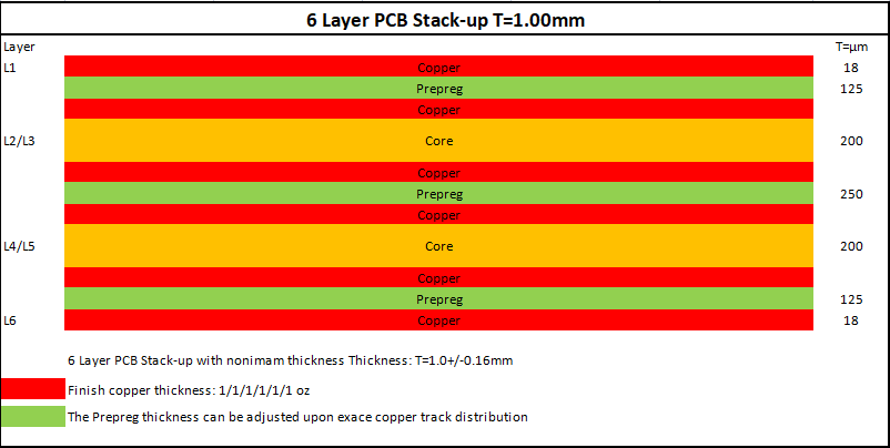
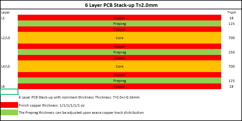
6-layers PCB is widely used in compact electronics such as communication modules, wearable devices and military equipments. There are high restrict engineering requirements of manufacturing particularly in process of plating, laminating and drilling. NextPCB own rich experience in 6 layers PCB fabrication during past 15 Years. Here is the 6-Layer PCB Stackup from NextPCB:.


A PCB stack-up is the arrangement of the copper and insulating layers of the PCB. The arrangement of the layers is usually done by the PCB engineer or the designer according to the circuit's requirements. There is not a fixed stack-up design available for any multilayer board. The designers are free to arrange the layers of the copper and insulating material according to their required specifications. However, the arrangement of signal, power, and ground layer affects the electrical and insulating properties of the circuit board.
Under this section, we will cover some different stack-ups in depth along with their effects on the overall circuit.
In this stack-up, the top and bottom signal layers have been merged with power planes instead of providing power planes with an individual layer. This stack-up is a very basic stack-up. The designers, while working with high-speed to moderate or low-speed signals, choose this stack-up to isolate low-speed signals from high-speed signals by routing them on the top and bottom layers. The slow-speed signals are routed at the middle layers. The ground plane between signal layers provides isolation that prevents electromagnetic interference.
Routing analog and digital signals in the inner layers of the board is not recommended in this stack-up. As there is no isolation among the inner signal layers, the parallel signal traces of analog and digital signals will experience cross-talk among them.
This stack-up provides a lower dielectric constant at the top and bottom layers. Hence, this stack-up makes the board perfect for the circuits that require controlled impedance at the top and bottom layers. Due to controlled impedance, this stack-up is good to choose for circuits that experience high-frequency signals. The only drawback of this stack-up is the lower decoupling force among the power and ground planes. However, the lower decoupling force is negotiable somehow. To balance the decoupling force, layer-4 can be used for routing low-speed signals that are linked back to power (L-3), which will then have direct coupling with the ground plane (L-2).
In this stack-up, the signal layers are adjacent to ground planes. The adjacent signal layer and ground plane ensures minimum cross-talk among the signals. Further, the closely placed Power and Ground planes provide interplanar capacitance that is essential for providing rapid switching current that is required by modern logic to drive transmission lines and supply current to IC cores. This is an ideal stack-up while signal integrity is concerned. The only drawback of this stack-up is that you lose a signal layer.
Bottom Line: The layers (stack-up) arrangement of the PCB plays an important role in the operation of the circuit. The order of the different layers affects the output of the circuit in terms of electromagnetic interference, decoupling force, cross-talk, etc. The customized arrangement of the layers can help in achieving desired dielectric constant, controlled impedance, and signal integrity.
So, we have analyzed some PCB stack-ups earlier in this article, but the question is that irrespective of technical requirements and details, is there any standard PCB stack-up that can work well in all circumstances? The answer is yes.
Signal/GND/Signal/Signal/PWR/Signal is a standard 6-layer PCB stack-up. This is a standard 6-layer PCB stack-up does not mean it is suitable for every type of circuit. The circuits that utilize high-frequency signals and require controlled impedance will not go with this stack-up. For example, this stack-up does not provide enough shielding against electromagnetic interference (EMI). However, adding an additional ground plane can reduce electromagnetic interference and cross-talk among the signals. OR keeping high-speed signals on a layer adjacent to the ground plane can still make things tolerable for high-speed circuits.
The standard thickness of a 6-layer PCB is about 0.062 inches to 0.125 inches. The weight of the copper layer in the PCB plays an important role in the overall thickness of the 6-layer PCB. The copper layer's thickness is decided by considering the amount of current that has to flow through the board. The standard copper thickness on a PCB is 1.37 mils (1.37 thousandth of an inch); this thickness can vary depending on the unique requirements of the board.
The sandwich-like structure of a PCB is made up of 3 different materials. The copper, prepreg, and core (FR-4).
The material that is used for the copper layer is pure copper, which has a network of signal, power, and ground tracks on it.
The prepreg is a fiberglass material infused with epoxy resin; it is different from the core in a way that it is an un-cured OR partially cured material. In addition, the materials for prepreg are in a malleable state, which means that they can be easily shaped as thin sheets. However, it is a dielectric material (a material that works as an insulator) used mainly for binding the core and copper layers.
FR-4 is a glass-reinforced epoxy laminate material that is used as the core of the PCB. The PCB core is a fully-cured material, which means it is heated and compressed in curing ovens to melt the prepreg in order to bind the core with thin copper layers. The PCB core material provides strength to the PCB and is responsible for the various electrical and environmental properties. Such as fire extinguishing, dielectric constant, electromagnetic interference (EMI), etc.
In a 6-layer PCB, there is no restriction for using components. We can use any electronic component of our choice, including
Resistors: Resistors are responsible for controlling the flow of current in a circuit.
Diodes: In a circuit board, diodes are responsible for letting the current flow in only one direction.
Capacitors: The main purpose of a capacitor is to store electrical charge. However, On a double-layer or multilayer PCB, its other uses include power conditioning, signal coupling and decoupling, noise filtering, and remote sensing.
Transistors: The transistors as a 6-layer PCB component have two applications, the first one is to switch the electronic signals, and the second is to amplify weak signals.
Sensors: Sensors, as a 6-layer PCB component, are used to identify changes in the environment and respond accordingly. These changes could be physical and electrical.
Transformers: In a 6-layer PCB, transformers are used to convert Alternating Current (AC) to Direct Current (DC).
Connectors: The use of a connector is to connect a printed circuit board with the actual module or machine and supply power to electrical devices.
LEDs: LEDs emit light when current flow through them. On a 6-layer PCB, LEDs are usually used to notify something special.
On a 6-layer board, the arrangement of the signal power and ground planes depends on the unique requirements of the circuit. But some ground rules of electronics are needed to keep in mind while designing the stack-up.
As we know, high-frequency and high-speed signals cause cross-talk among the adjacent signals and signal layers. Therefore, it is necessary to route those signals in the inner layers of the board and provide shielding to the respected layer. By shielding, I mean giving a layer of the core, prepreg, or ground plane among the high-speed and high-frequency signals to isolate them to decrease cross-talk and electromagnetic interference (EMI).
Signal/GND/Signal/PWR/GND/Signal is an ideal arrangement of layers and planes for a high-speed circuit. The top and bottom layers are good to dedicate to the high-speed or high-frequency signals as those layers are perfectly isolated and provide a low dielectric constant.
A mixed circuit refers to a circuit that uses both analog and digital signals. The previously mentioned stack-up Signal/GND/Signal/PWR/GND/Signal is an ideal stack-up for mixed circuits, as, in this stack-up, the top and bottom signal layers are adjacent to the ground plane. The analog and digital signals can be routed on each outermost layer of the PCB as both layers are well shielded and have a solid reference plane on the opposite side of the board. Due to this, there will be no impedance mismatches, excessive inductance, and radiated noise among the signals.
Bottom Line: The arrangement of the layers and planes on a 6-layer board should be made in a manner that provides maximum shielding to the high-speed and high-frequency signal layers. There is not any fixed stack-up available that is suitable for every type of circuit. The designers should have a good understanding of the circuit's requirement to produce a well-functioning printed circuit board.
There are several factors that determine the design of a 6-layer PCB stack-up. Some of them are
The key factors in determining the stack-up design of a 6-layer printed circuit board are where the circuit has to be used and its application. Every individual domain where the PCB has to be used demands distinct electrical and environmental properties. To meet the distinctive requirements of the circuit and achieve the required output, designers and engineers arrange the layers and planes by considering the unique requirements of the circuit board.
For example, a low-speed circuit with a wide range of signals to route requires more signal layers, while on the other hand, a high-speed or high-frequency circuit requires more shielding to protect signal integrity. In order to do so, a signal layer is sacrificed to add an extra ground plane.
Design configuration refers to the hardware details of the PCB. Such as the size of the PCB and the quantity of holes we can have on a PCB. These details help in determining the PCB stack-up. The design configurations are usually different for individual circuits. Therefore, understanding design configuration before deciding on the stack-up and routing tracks is crucial to avoid unwanted issues later.
Electrical specifications include dielectric constant (DK), dielectric breakdown, impedance and coefficient of thermal expansion, etc. Based on the arrangement of the layers, the electrical properties of the board vary. Such as keeping outermost layers adjacent to the ground plane provides a low dielectric constant and reduces electromagnetic interference (EMI). In a nutshell, the specifications of a circuit help the designer to select the stack-up design which meets these electrical specifications to get the required output.
To increase component density, experienced designers use both sides of the PCB instead of cramming a single side with too many components. To do so, the designers need to connect those components on different layers with each other, which they do by using PCB vias. The hidden and blind vias help in connecting different layers of the PCB. The use of vias to increase component density can affect the design of the 6-layer PCB stack-up. Because vias have inductance. In high-speed circuits, the inductance of vias can make a difference in signal integrity and affect the stack-up design.
The price determination of a 6-layer printed circuit board depends on the three factors
The quality of the material is chosen by the designer or the PCB manufacturer. High-quality material burdens the budget more. The size and quantity of the PCB is another factor that determines the cost of a 6-layer PCB. PCBs that are ordered in bulk or at least somewhere about ten or more pieces cost a bit lower if compared to the price of a single PCB. The thickness of the copper layer of the PCB, which is decided by the flow of current that has to pass from the circuit, is a major player in the cost determination of the 6-layer PCB. As the number of layers is large, a minimal change in the thickness of the copper layer can hugely fluctuate the prices.
In some exceptional cases, to increase the temperature resistance of the PCB, we need to customize the normal core material (FR-4) in terms of resin. This customization of FR-4 base material increases the price of PCB production.
The sizes of holes and their dimensions affect the whole production cost of the board. The greater the quantity of the holes, the more time requires for the manufacturing process. Further, the dimensions of the holes matter a lot. Because the smaller holes require more special machinery and time to drill, it ends up affecting the overall manufacturing cost of the PCB.
> Recommend reading: How to Choose a China Circuit Board Manufacturer (2025 Guide)
A standard 4-layer PCB provides 2 signal layers, a power plane and a ground plane. On the other hand, a 6-layer PCB provides 3-4 signal layers to route tracks, a power plane, and 1-2 ground planes. In any multilayer printed circuit board, the number of layers and planes is not fixed but decided by the designer by considering the unique requirements of the circuit. In 6-layer and 4-layer PCBs, the difference not only revolves around their number of layers, but the main difference occurs when it comes to their area of application, cost, and performance.
The performance of a 6-layer PCB is higher as it provides improved electromagnetic interference (EMI) and better opportunities to route high-speed and mixed signals. In a 6-layer PCB, it is easy to achieve low EMI by keeping the signal layer adjacent to the ground planes, which ensures signal integrity. Further, a well-designed 6-layer PCB stack-up can prevent issues caused by cross-talk and reduce the impact of external noise on the circuit. Which eventually increases its performance over 4-layer PCB.
Due to the increased number of copper, prepreg, and core layers, the cost of a 6-layer PCB is higher than the price of a 4–layer PCB. However, the number of layers is not the only reason for the high cost of a 6-layer PCB. But, the number of holes, their dimensions, and vias present on a board also affect the cost of a 6-layer PCB.
In many cases, we can easily avoid a 6-layer PCB by routing the signals wisely on a 4-layer board. But there are some domains where signal integrity is crucial. The signal integrity and electrical requirements of individual circuits are different, which helps the designers to choose between a 4-layer and a 6-layer PCB. Some common areas of application of a 4-layer PCB are consumer electronics and low to moderate speed circuits. Whereas a 6-layer PCB is good to use for high-speed and high-frequency circuits that require controlled impedance and a lower dielectric constant.
The applications of a 6-layer PCB are wide. But they are mainly used in
The manufacturing process of a 6-layer PCB is divided into several steps.
NextPCB is one of the global leader in PCB manufacturing, known for delivering high-quality PCB products and exceptional customer service. With over 15 years of experience, we specialize in producing everything from single-layer to multilayer boards. Our expertise and commitment to quality have earned us a reputation as one of the top 6-layer PCB manufacturers worldwide. NextPCB offers custom 6-layer printed circuit boards, complete with assembly and testing, tailored to your specific requirements.
In addition, NextPCB provides a range of services, including component sourcing, PCB prototyping, manufacturing, assembly, quality testing, and final delivery. Simply put, NextPCB can fulfill all your needs, from initial prototyping to both small and large-scale PCB production.
>>Get a quick online PCB quote within 24 hours.
A 6-layer printed circuit board provides higher performance and durability. In addition, a well-designed 6-layer PCB stack-up ensures signal integrity and a low dielectric constant (DK). The designing and manufacturing process of a 6-layer PCB is complex and time taking. But a 6-layer PCB provides more opportunities to route Signals, Power, and Ground tracks on a smaller surface.
The stack-up design of a 6-layer PCB depends on the unique requirements of individual circuits. Therefore, deciding the stack-up or arrangement of the layers by acknowledging the requirements of the board provides better electrical properties. For example, reduced electromagnetic interference EMI, cross-talk, and lower impact of external noise.
The difference between a 6-layer and a 4-layer PCB is not huge. If the stack-up and layout of a 4-layer PCB are designed carefully and judicially, a circuit designed on a 6-layer PCB can be designed on a 4-layer PCB. However, we will deprive some electrical specifications in this scenario.
The price of a 6-layer PCB depends on several factors, such as the thickness of copper layers, base material, and other factors. But the size of the PCB, the number of holes, and their dimensions play an important role in the price determination of the PCB.
Still, need help? Contact Us: support@nextpcb.com
Need a PCB or PCBA quote? Quote now


 Printed Circuit Boards
 Surface

