
 NextPCB Capabilities
Printed Circuit Boards
NextPCB Capabilities
Printed Circuit Boards
 PCB Assembly
 Layer Buildup
 SMD-Stencils
 PCB Design-Aid & Layout
 Mechanics
 Quality
 Drills & Throughplating
 Factory & Certificate
 PCB Assembly Factory Show
Certificate
PCB Assembly Factory Show
Certificate
Support Team
Feedback:
support@nextpcb.com


A 4-layer printed circuit board is an electronic card, usually green in color, that provides four conductive layers to route electronic signals. The number of layers in a standard 4-layer PCB consists of two routing layers, one power, and one ground layer.
A solid reason for moving to a 4-layer PCB is that it helps surpass the limitations of a 2-layer PCB. The added two layers assist in achieving multiple electrical characteristics such as ideal impedance, maximum shielding to signal layers, and increased electromagnetic compatibility (EMC). 4-layer PCBs allow routing of more complex circuits on a shorter surface. Further, it helps in achieving signal integrity and reduces EMI issues.
Despite the exceptional performance and durability, a 4-layer PCB has some drawbacks. One of which is its high cost. A 4-layer PCB almost costs double that of a 2-layer PCB.
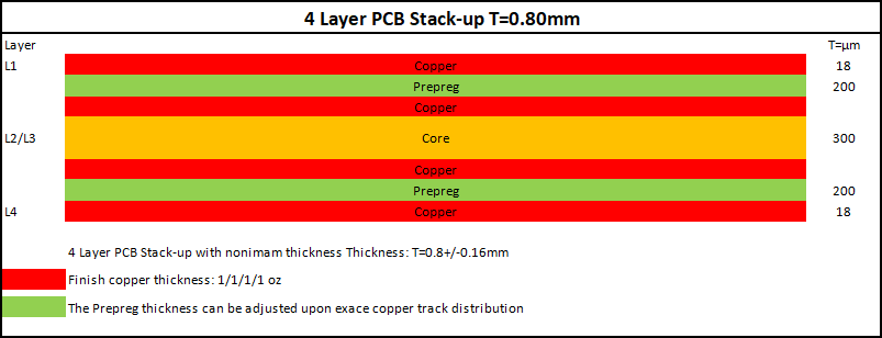
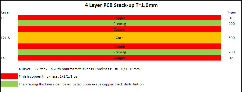
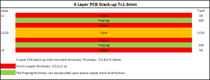
A 4-layer PCB stack-up is the arrangement of layers along with the determination of the base material and thickness of the final board. The stack-up design intends to eliminate uncertainties regarding the material and electrical properties. Before designing the layout and deciding on the number of planes, the required isolation and routing technique always helps in understanding the requirements of the board, which is necessary to produce a well-functioning PCB. NextPCB usually provides five standard PCB stack-ups with various thicknesses; they are as under.


A PCB stack-up refers to the arrangement of conducting and insulating layers of a PCB. The engineer or the designer usually does the stack-up design of a 4-layer PCB by considering the requirements of the circuit. The stack-up influences the electrical properties of a circuit, and therefore, the arrangement of the layers according to the circuit’s requirements helps in achieving the desired results. Whereas a small mistake in the stack-up design can lead to problems such as electromagnetic interference, poor signal integrity, and crosstalk.
>> Recommend reading: How to Design a 4-Layer PCB Stackup for High-Speed Digital Circuits
In this section, I will briefly define some stack-up designs with their individual qualities and suitable conditions to use.
Signal/Ground/Power/Signal is a commonly used PCB stack-up. This stack-up, due to adjacent power and ground planes, provide ideal impedance and shielding to the signal layers. A separate power plane in this stack-up assists in reducing volt drop.
The maximum shielding between signal layers makes this stack-up ideal for high-speed, high-frequency, and mixed-signal circuits. As we know, the ground plane absorbs high radio-active waves. So it is ideal for keeping the ground plane adjacent to the signal layer that uses more high-frequency signals. But nothing is perfect! The drawback of this stack-up is the use of excess vias to connect signal traces to the ground plane.
Not a commonly used stack-up. But dedicating outermost layers to the ground plane provides high Electromagnetic Compatibility (EMC), which increases the ability of a circuit to work under an electromagnetically affected environment. Further, this stack-up helps to reduce the impact of external noise on the board. The drawback of this stack-up is that there is no shielding between the signal layers which increases the risk of crosstalk, volt drop, and EMI issues. Hence, poor signal integrity.
However, if the circuit demands external shielding, we can work on reducing the crosstalk by routing the signal tracks perpendicular to different layers. But still, it does not make the circuit ideal for high-frequency signals.
This stack-up is ideal for high-frequency boards (the frequency that ranges in GHz). Both signal layers are perfectly isolated from each other. Hence, no crosstalk and EMI issues. The two adjacent ground planes make this stack-up perfect for circuits that require controlled impedance.
The drawbacks of this stack-up include fewer surface-to-route signals and poor isolation from the external environment.
Bottom Line: The stack-up design of a PCB is the most crucial part of PCB design and manufacturing, which depends on the individual requirements of the circuit. When designing a PCB stack-up, the characteristics of a board should be considered. For example, High-frequency, High-speed, and mixed circuits require more shielding from inner layers to eliminate crosstalk and EMI issues, whereas some circuit designs require isolation from external noise. So, their stack-ups should also meet these needs of the circuits. Otherwise, negligence in choosing the material and right stack-up can lead to issues later.
Signal/Ground/Power/Signal is a standard 4-layer PCB stack-up. By standard, it means that this stack-up is a frequent choice of multiple designers. An advantage of using standard stack-up is that the manufacturers do not ask for higher prices for the PCB as they do not have to do anything unusual that raises the manufacturing time and their efforts in the fabrication process of your board.
A standard 4-layer PCB stack-up is mostly a reliable choice for multiple designers. But this does not mean that you can choose a standard stack-up for every circuit. The standard stack-ups are ideal for boards that do not have complex requirements. If your PCB demands some unique electrical characteristics and operating conditions, such as if it utilizes high-frequency signals or requires shielding from external noise. Please prefer to choose a custom stack-up to avoid unnecessary issues later.
The standard thickness of a 4-layer printed circuit board ranges from 0.020", 0.031", 0.040", 0.047", 0.062", 0.093" to 0.125". The thickness of a 4-layer PCB depends on the thickness of copper, prepreg, and core material. Every individual board has unique requirements for the thickness of used material, such as the circuit boards that require more isolation demands thicker core(s) and prepregs. Designers and engineers decide the thickness of a PCB by considering several factors, such as design configuration, heat dissipation qualities, and electrical requirements of the board. Briefly, the thickness of a 4-layer PCB is not fixed. Hence, you should always confirm with the PCB manufacturer if they provide your required thickness.
The 4-layer printed circuit boards used a variety of materials depending on their applications. The total number of materials used in a PCB is four, consisting of copper, prepreg, core, and solder mask. A brief description of the material is as follows.
The copper layer is the only current conducting layer of the printed circuit board used to route signal, power, and ground traces. The standard copper thickness of a 4-layer PCB is 1.37 miles (1.37 thousandth of an inch). But the weight of the copper layer can vary depending on the operating current of the PCB. In an ideal condition, the higher current a PCB goes through, the thicker should be the copper layer.
The Prepreg is a dielectric material made up of fiberglass infused with epoxy resin, mainly used for binding and isolating copper layers from each other. The PCBs used a variety of Prepreg thicknesses depending on the isolating requirements of the individual layers.
The solder mask is a thin liquid epoxy or polymer material applied on the outermost layers of the PCB to prevent PCB tracks from oxidation and shorting. Another primary function of the solder mask is to resist the formation of solder bridges among closely spaced solder pads.
The PCB core functions as the base of a printed circuit board and hence, a wise selection of core material is essential as it influences the electrical properties such as fire extinguishing, dielectric constant, electromagnetic interference (EMI), etc., and mechanical strength of the board.
A wide range of PCB core materials known as PCB substrates is available. However, the choice of the PCB substrate depends on the unique requirements of the board.
Here, we are discussing some commonly used PCB substrates. So, you get a rough idea about the variety of substrates and the suitable conditions to use them.
FR-4 is a flame retardant glass-reinforced epoxy laminate and a standard for PCB substrate. This material's electrical and environmental properties are excellent for a general-purpose PCB. Along with being fire retardant, this material provides high water resistance, which makes it a perfect material for marine application. Despite all of its properties, FR-4 is the lowest-cost PCB substrate.
Related: Guide to FR-4 Printed Circuit Board (PCB) Material - NextPCB (Link this)
Metal core PCBs use Aluminium, copper, or steel as the base material. These PCBs provide high heat dissipation and mechanical strength to the board, which is excellent when using really-heavy components. The Aluminium core PCBs are higher in cost than Copper core PCBs. That's why Copper core PCBs are more common to see.
Ceramic PCBs use ceramic-based materials such as aluminum nitride and beryllium oxide as base material. The heat dissipation property of a ceramic PCB substrate is higher than any other PCB substrate. Other qualities of the ceramic substrate include excellent high-frequency performance, high durability and reduced crosstalk.
Composite Epoxy Material is made up of woven glass fabric surfaces and non-woven glass core impregnated with epoxy resin.
High-Frequency Laminates
High-frequency laminates are very useful for high-frequency applications. The properties of this laminate eliminate other core materials when signal integrity and impedance are concerned.
High-frequency laminate provides a stable dielectric constant, controlled impedance, and eliminates crosstalk. Hence, considered an ideal substrate for high-frequency boards. High-frequency laminate is a costly material, but its properties justify the cost.
A component is any device that influences the flow of electrons and their field in an electronic system. As per the definition of a component, any type of component is acceptable to use in a 4-layer or other PCBs. Some widely used electronic components are:
The arrangement of the ground and power planes depends on the electrical requirements of the board. In a 4-layer printed circuit board, we can dedicate two layers to have individual power and ground planes. But in some cases, the designers can merge the power plane with the signal layer. As the maximum number of planes we can have in a 4-layer PCB is two, their arrangement can influence the performance of the PCB. Hence, considering some scenarios is better to build a firm understanding to decide the best possible ground and power plane arrangement for your circuit.
The first possibility of arranging power and ground planes in a 4-layer PCB is to keep both power and ground planes adjacent by routing them in inner layers. In this way, the closely placed planes will provide interplane capacitance, which is beneficial for rapid switching. Further, this arrangement will shield the top and bottom layers maximum, eliminating crosstalk. But this arrangement has its drawbacks. The outermost layers will not have any protection from the external environment. For example, the boards that operate in a high electromagnetic environment require shielding against their surroundings to operate without electromagnetic interference (EMI) issues. Another issue with this stack-up is that the designers will need to put excess vias to connect the signal layer (adjacent to the power plane) to the ground plane.
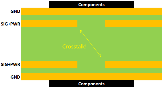
The second possibility to arrange the signal, power, and ground plane is to sandwich the signal layers between two ground planes and combine the power tracks with the signal layers instead of dedicating a separate layer. This arrangement will provide maximum shielding against the surrounding of the board. But this order of the layers does not provide shielding to the signal layers, which can be a big turn-off while working with high-speed boards as it will create massive crosstalk among the signals. However, we can still use this stack-up for low to moderate-speed circuits by increasing the thickness of Core and Prepreg to increase shielding. Further, routing the signals perpendicular to the two layers can also be beneficial perpendicular which means routing tracks horizontally on the first layer and vertically on the second layer to reduce crosstalk.
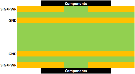
Sandwiching two ground planes between two signal layers is the best arrangement of layers for the high-speed, high-frequency and mixed circuit boards. This stack-up provides maximum shielding between the layers with ideal impedance. Hence, no crosstalk and EMI issues.
Bottom Line: The number of layers in a 4-layer PCB is less. Hence, their proper arrangement is crucial for achieving the required electrical and mechanical properties. In a 4-layer PCB, we can either have one power and one ground plane or two ground planes with two signal layers combined with power tracks. However, we should choose the stack-up or arrange the layers according to the unique requirements of the board.
Several factors that determine the design of a 4-layer PCB stack-up include
The application area may refer to the environment and industry in which the PCB has to operate.
The purpose of a PCB and its operating environment always have a powerful impact on the stack-up design. For example, if a PCB has to operate high-speed and high-frequency signals, the stack-up must use a thicker core and Prepreg as well as provide adjacent ground to the high-speed layers. Whereas, if the board has to operate under specific environmental conditions, the material of the board and arrangement of the layers should have done by considering those conditions. For example, if the board operates under high temperatures, the choice of the material should be accordingly. OR if the board has to work under high external noise, the outermost signal layers should not leave exposed. It's better to shield them with the ground plane.
The design configuration cites the hard details of a system or board, such as the height, size etc. In some cases, there is a size limit for the printed circuit board because the device has limited space for the PCB. In such cases, the designers should be cautious while deciding the number of layers and their arrangement because any error at this stage can be critical later. The design configurations for the PCBs are usually different for distinct boards, but they are dominant enough to consider while concluding the stack-up design. Let's understand this with an example; you are designing a PCB for a handy gadget with size limitations and a complex routing design, which has many signals to the route. Now, in this case, you have to handle the number of signal layers and manage the ground and power plane to meet the design configuration without running out of space and compromising signal integrity. That's where design configurations come into play.
The stack-up design of a PCB solely depends on the electrical specifications of the board. The electrical specifications of a circuit set the priorities for the order of power, ground and signal layers.
Even the thickness and type of core and prepreg material depend on the electrical specifications of the circuit. Because, along with a good layout design, the type of material and the stack-up design, everything works together to achieve the desired output.
The 4-layer PCB costs double that of a 2-layer PCB, and the designers also charge extra to design them as they spend more time and effort on a 4-layer PCB. Despite the number of layers of the PCB, a complex design with precise details and non-standard stack-ups increases the production and designing costs. That’s why the designers should try to design the PCB as simple and close to the market standard as they can.
The component density refers to how dense a board is with components. Of course, components do have weight. They carry space and many pins/terminals to route on the PCB. So the number of components has a lot to do with the PCB strength, size of the board, and its frequency limitations. Hence, the component density is considered an important factor in determining the stack-up design.
The price of a printed circuit board is never the same or fixed. Different manufacturers charge individual prices based on the properties of the PCB. But still, some factors help us to estimate the cost of the 4-layer PCB (For a detailed discussion on optimizing PCB costs during design, see Custom PCB and PCBA Cost Analysis). Some of them are as below.
An engineer's responsibility is to choose the best possible quality of the printed circuit board material by considering the PCB requirements. A little compromise in the material can destroy the base, and a building is without the base. However, it is clear that high-quality material increases the price. Further, the thickness of the material, size, and quantity of the boards also fluctuate the manufacturing cost. A single PCB with more precise requirements costs higher in manufacturing as it requires the manufacturer more time to produce a single piece of PCB while using all of their equipment at max.
Under some precise circumstances, the PCB requires high-temperature resistance to maintain its performance. Some PCBs either work in a hot environment or their components produce more heat than the heat managing capacity of the material, due to which the excess heat starts damaging the PCB surface and signal tracks. To deal with this condition, the engineers suggest modifying the heat resistance capacity of the material in terms of resin which adds up the cost.
The order of a standard 4-layer PCB splits into two signal layers, a power plane, and a ground plane. However, a standard 6-layer PCB provides three signal layers and three layers dedicated to the ground and power plane. Physically it’s hard to point out any difference between them. But electrically, both PCBs have a massive difference in terms of performance, cost, and application area.
A 6-layer PCB is higher in the number of layers, which helps provide shielding among the signal layers and sometimes from the external noise. A separate power plane on a 6-layer PCB helps to minimize volt drop and operate a high current. In a 6-layer board, the designers can try different stack-ups to meet their needs. On the other hand, a 4-layer PCB is good enough for moderate types of boards, and designing a complex circuit with lots of signal tracks and especially high-frequency signals can cause issues like crosstalk and electromagnetic interference. In terms of performance, a 4-layer PCB is a good option for moderate-speed circuits with not-so-massive routing and special environmental/electrical conditions. However, designing the stack-up and layout with devotion can help surpass the performance limits of a 4-layer PCB and achieve the desired results.
A standard 4-layer printed circuit board costs lesser than a 6-layer PCB. But this can not be true necessarily, as the cost of a PCB depends on several factors, such as the quality and thickness of materials, etc. So, according to this, the prices of a complex and enhanced 4-layer PCB may reach the cost of a standard 6-layer PCB.
4-layer PCBs provide enough surface to design most of the circuits. Many electronic appliances are using 4-layer PCBs to meet their requirements. They include
The manufacturing process of a 4-layer PCB includes several steps.
That is all the PCB is ready to use.
NextPCB is one of the experienced manufacturers of PCB around the globe, providing high-quality PCB products with dedicated customer service. We have been manufacturing single-layer to multilayer boards for more than 15 years. Our experience and quality of work have given us the confidence to count Next PCB as one of the best 4-layer PCB manufacturers around the globe. We are manufacturing all the PCB stack-ups written above and other stack-ups provided by our honourable clients. Further, Next PCB can provide an assembled and tested 4-layer printed circuit board on your demand.
The other services of Next PCB include components sourcing, PCB prototyping, PCB manufacturing, PCB assembly, quality testing, and the final shipment. Briefly, NextPCB can meet all your PCB requirements, from PCB prototyping to small or mass PCB production.
>>To get a quick online PCB quote within 24 hours.
The standard 4 layer PCB cost as low as $13 for 5-10 pieces, however, new customers, 4 layer PCB cost as low as $3 for 5-10 pieces: fr-4, size not over 100mmx100mm, 1oz. Order Now
A 4-layer printed circuit board provides good shielding and power management for a not-so-complex circuit, and the individual power plane gives better volt drop resistance.
In a 4-layer PCB, the opportunities for routing high-frequency and mixed signals are way more than in a 2-layer PCB. Though a 4-layer PCB has some electrical limitations, we can surpass these limitations with a more precisely designed stack-up.
Further, the performance and durability of a 4-layer PCB are more than a 2-layer PCB but less than a 6-layer PCB. The same goes for the price of a 4-layer PCB.
Still, need help? Contact Us: support@nextpcb.com
Need a PCB or PCBA quote? Quote now


 Surface

