
 NextPCB Capabilities
Printed Circuit Boards
NextPCB Capabilities
Printed Circuit Boards
 PCB Assembly
 Layer Buildup
 SMD-Stencils
 PCB Design-Aid & Layout
 Mechanics
 Quality
 Drills & Throughplating
 Factory & Certificate
 PCB Assembly Factory Show
Certificate
PCB Assembly Factory Show
Certificate
Support Team
Feedback:
support@nextpcb.com


A 10-layer PCB is an electronic circuit that provides 10 conducting layers to route signal traces; it is more than enough to route a complex circuitry with quality features. The layers in a 10-layer board can easily stack according to the requirements of the individual circuits, which eventually help to achieve desired electrical properties.
A 10-layer PCB stack-up is the arrangement of layers along with the determination of the base material and thickness of the final board. The stack-up design intends to eliminate uncertainties regarding the material and electrical properties. Before designing the layout and deciding on the number of planes, the required isolation and routing technique always helps in understanding the requirements of the board, which is necessary to produce a well-functioning PCB.
NextPCB usually provides five standard PCB stack-ups with various thicknesses; they are as under
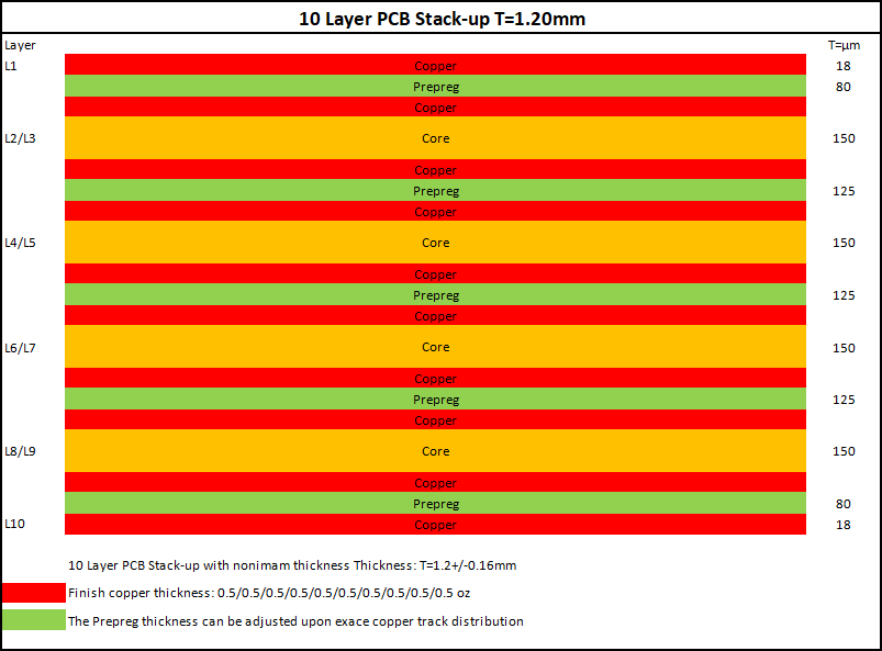
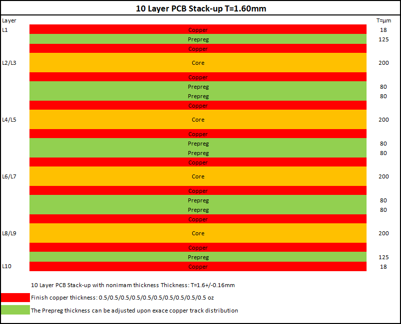
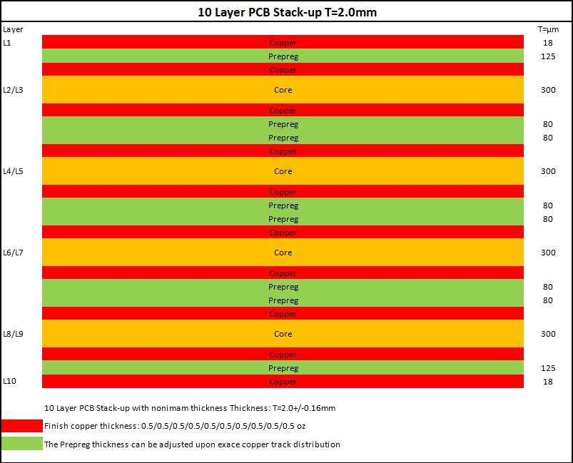
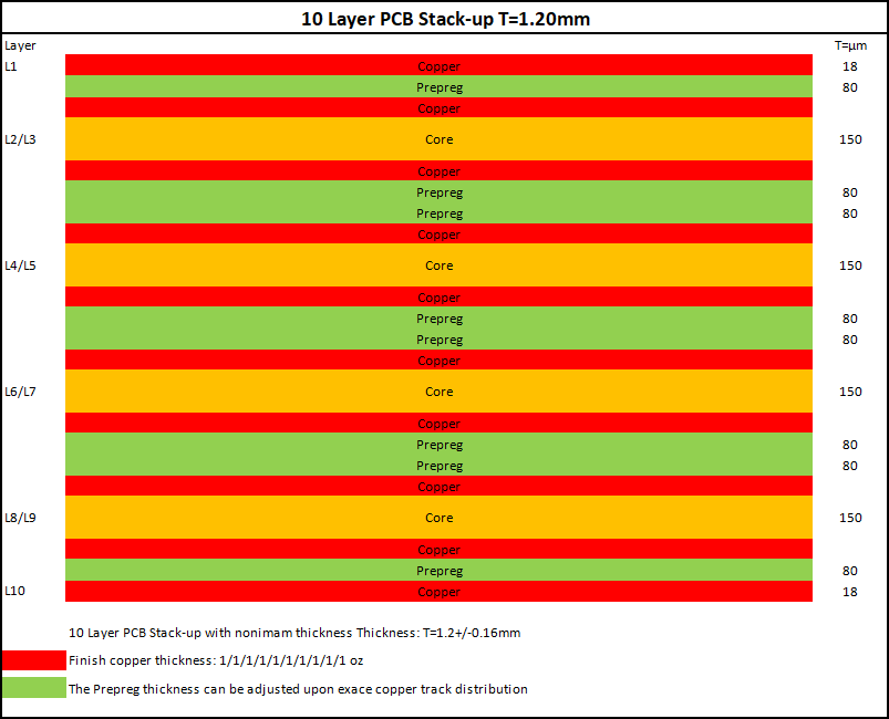


Bottom Line: The above are only standard 10-layer PCB stack-ups that are widely used in the market. But the designers can choose the thickness of the material according to the isolating requirements of the individual boards. A PCB with a special thickness of material and glass transition temperature (Tg) usually costs more than the standard PCBs. To get a quick quote within 24 hours on your 10-layer PCB with special features, contact NextPCB.
All the above-mentioned stack-ups are standard stack-ups for a 10-layer PCB. Though, the second stack-up with a core thickness of 210um is the most widely used stack-up as this stack-up meets the isolation requirements for general-purpose PCBs. An advantage of using a standard 10-layer stack-up is that the manufacturer does not need to go beyond their regular schedule to fabricate the PCB, which cut-of the extra manufacturing cost and delivery time.
The standard 10-layer PCBs are available in the thickness range from 1.33mm to 3.0mm. However, the thickness of a 10-layer PCB depends on several factors, such as the thickness of copper, prepreg and core. The PCBs with high requirements of isolation may use double layers of prepregs, whereas for operating high currents without damaging the signal traces, the thickness of copper material can reach up to 105um (3oz) or more. Such factors play a significant role in determining the thickness of a 10-layer PCB.
The sandwich-like structure of a PCB mainly consists of 4 different materials. The copper, prepreg, core, and solder mask.
Copper is the conducting material of the 10-layer PCB. If the 10-layer PCB is utilizing high-current or generating a large amount of heat, the amount of copper on the outer layers can be as thick as 3oz to fasten the heat dissipation and handle the current without significant loss and damage to the PCB.
Prepreg is a dielectric material used to bind the PCB cores together or with copper layers. The thickness of prepreg also determines the isolation among the signal layers.
The solder mask is a liquid epoxy material applied to create a barrier between the external copper layers and the environment. Solder mask on the outer layers of the PCB prevents shorts and open circuits.
A core is the base material of a 10-layer PCB; that provides mechanical support and isolation. Due to distinct requirements of electrical and mechanical properties, PCBs use several types of materials as the core; these materials include
FR-4 is a standard material used as a PCB core. The huge demand for FR-4 material makes it the most affordable material and reduces the delivery time of FR-4 PCBs. The glass transition temperature of FR-4 material is as high as 180C, which might make it an undesirable material for high-temperature applications, but this material has the property to extinguish the fire on itself.
Metal core PCBs use metals such as Copper and Aluminum as the base material. The PCBs that require high-glass transition temperature, extra mechanical strength and higher dissipation rate should use Metal core to meet their requirements.
Ceramic PCBs use aluminum nitride and beryllium oxide as the base material, which provides high thermal conductivity, minimal coefficient of thermal expansion (CTE), and stable dielectric constant (DK), which help in minimizing signal loss.
High-Frequency Laminates are excellent for circuits that need a faster signal transmission, controlled impedance, low signal loss and least dielectric constant (DK) and dissipation factor (DF). Hence, high-frequency laminates are exceptional for circuits with special requirements and critical applications.
The production cost of the PCB depends on its design, the PCBs with complex designs and non-standard techniques cost more than standard PCBs. We are enlisting five factors that have a high impact on the cost of a 10-layer PCB
The standard PCBs use FR-4 as a base material. But PCBs designed for high-tech devices that operate high-frequency, high-speed signals or require high-temperature resistance need high-quality materials such as Rogers and PTEF. High-quality materials are higher in price, and with the large dimensions of boards, the amount of material and fabricating time increased, which impacts the PCB cost.
The extra thin holes require special machinery and skills to drill. Other unique features in a board, such as the thickness of prepreg and solder mask and edge plating, contribute to the price determination of the PCB.
A 10-layer PCB can use all components; some of them are as follow
Because a 10-layer PCB has more layers than 2-layer and 4-layer PCB, the arrangement of layers and planes is easy, as there is no shortage of space. What we need to focus on are the fundamental rules of PCB designing.
There is plenty of space to route signal traces, but routing is not the only goal to achieve, but what is crucial is to maintain the signal and power integrity.
Whenever deciding on the arrangement of the signal, power and ground layers focus on these things.
The faster the signal, the higher electromagnetic interference it can create if it does not have a direct current return path. In this situation, having a plane adjacent to signal layers is beneficial as it provides direct return paths and shields the layers against cross talk.
To reduce volt drop in a 10-layer PCB, try to have at least one power plane that is best if adjacent to the layer with the highest-frequency signals.
If the PCB has to operate under a high electromagnetic environment, consider dedicating the top and bottom layers as a ground plane to shield the circuit from external electromagnetic interference.
A considerable stack-up for a low to medium frequency 10-layer PCB is
The design of a PCB (including stack-up and layout design) depends on several factors; it gets changed with the requirements and operating conditions of the PCB. Some of the main factors that influence the overall design of the PCB are
The area of application is the main factor that determines the design of the PCB because each domain has specific requirements. For example, high-frequency circuits require extra shielding, whereas PCBs that operate under an electromagnetic environment require higher electromagnetic compatibility. These differences in their working domains define their characteristics, which are crucial to follow during the designing stage of the PCB to get an accurately functioning PCB.
The PCB is a part of a module. If the module has specific conditions for the PCB, its design should follow those conditions. For example, if the module lacks space and can not fit a rigid PCB. The designers can find a substitute for rigid PCBs in flexible PCBs, which are proven more reliable against continuous mechanical pressure and vibration. Other hardware configurations also affect the PCB design in various terms, but the designers can tackle these obstacles by modifying the design and following the best PCB designing practices.
electrical specifications of the board, such as signal integrity, electromagnetic compatibility and heat dissipation requirements of the circuit, also affect the design of the PCB in terms of the quality and thickness of material and routing style.
The PCBs with specific electrical requirements usually demand unusual time and machinery at the fabrication stage. The designers also charge extra for integrating special features. To manage the manufacturing cost of the PCB, the designers try to keep the PCB design as near to the standard design as possible.
Component density plays a significant role in deciding the layers of the PCB. The higher the components, the larger space required to manage their leads and route them. In this case, having multiple layers to route signals prevents parallel, long traces.
There is an enormous difference in the layers of a 4-layer and a 10-layer PCB. Hence, in the performance and cost. A 10-layer PCB provides many opportunities to divide the structure between signal layers and planes. This feature of a 10-layer PCB improves its performance as power and ground planes provide shielding, return path for current and reduce volt drop. If concerning electromagnetic compatibility, a 10-layer PCB is more reliable than a 4-layer PCB.
The cost of a 10-layer PCB is more than double that of a 4-layer PCB.
A significant downside of using a 10-layer PCB over a 4-layer PCB is its high design and manufacturing cost.
There are numerous advantages of a 10-layer PCB; they include
10-layer PCBs have applications in most sensitive devices and machines, including military and aerospace devices. A list of application areas of 10-layer PCB is as under
The manufacturing process of a 10-layer PCB starts from the testing of the layout file and has several stages after it,
1. As we stated, the first stage is to check the layout file and approve it for further process.
2. The approved files then go for the printing of photo tools, which is a process of converting copper traces onto films by using a plotter.
3. Then the photo tools are converted onto the laminates, which are thick sheets of base material coated with copper.
4. Then these PCB laminates undergo pressure wash, which uses a strongly alkaline material to etch excess copper from the laminates.
5. After the pressure wash, the laminates go for automatic optical inspection to identify errors. At this stage, identifying errors is essential as it is impossible to modify the laminates once they are stacked.
6. The next step is to punch registration holes which helps in aligning all the laminates, prepreg and copper sheets together on the binding stage.
7. Now, on a base of steel, all the laminates, prepreg sheets, and top and bottom copper layers are stacked one by one and aligned using previously punched holes.
8. Once everything is stacked and aligned, the manufacturer placed the top part of the steel plate and screwed the top and bottom steel plates together.
9. Then this stack-up undergoes a specific pressure and heat. The heat melts the prepreg, and pressure helps to bind all the laminates and copper layers.
10. After the binding of the layers, the manufacturer prints and prepares the top and bottom layers by following the same process as the inner layers.
11. Then the stack-up needs to drill holes and vias that need to deposit with some conducting material as the prepreg and laminates are non-conductive.
12. Once the electroplating is done, the PCB is ready for a coat of solder mask and then silk screening to print the required information on the outer layers of the PCB.
13. The last stage of PCB manufacturing is to test the PCB against the layout file and deliver it to its owner if there are no issues.
NextPCB has been providing high-quality tested 10-layer PCBs for more than 15 years. We are manufacturing a wide range of 10-layer PCBs with different base materials and special manufacturing requirements. Quality is the foremost priority of NextPCB. Hence, we perform several tests on our manufactured 10-layer PCBs to ensure the delivery of a flawless PCB. The NextPCB provides all the stack-ups mentioned above. But if you need a custom-made multilayer PCB with unique specifications and a particular manufacturing process, contact us to get a quick quote within 24 hours.
A 10-layer PCB is a high-performance and durable electronic circuit board with several prominent features. A characteristic of a 10-layer PCB is that it provides numerous stack-up options that help to cover a wide range of special requirements. The price of a 10-layer PCB depends on several factors, such as the thickness of the PCB, type of material and manufacturing process. A 10-layer PCB provides good electromagnetic compatibility and reduces EMI issues. But, for high-frequency boards, a 10-layer PCB with standard FR-4 material is not compatible enough. But, with high-quality base materials like Rogers and PTEF, a 10-layer PCB can be excellent for several sensitive and high-performance demanding industries, such as military, aerospace and telecommunication.
Still, need help? Contact Us: support@nextpcb.com
Need a PCB or PCBA quote? Quote now


 Surface

