
 NextPCB Capabilities
Printed Circuit Boards
NextPCB Capabilities
Printed Circuit Boards
 PCB Assembly
 Layer Buildup
 SMD-Stencils
 PCB Design-Aid & Layout
 Mechanics
 Quality
 Drills & Throughplating
 Factory & Certificate
 PCB Assembly Factory Show
Certificate
PCB Assembly Factory Show
Certificate
Support Team
Feedback:
support@nextpcb.com


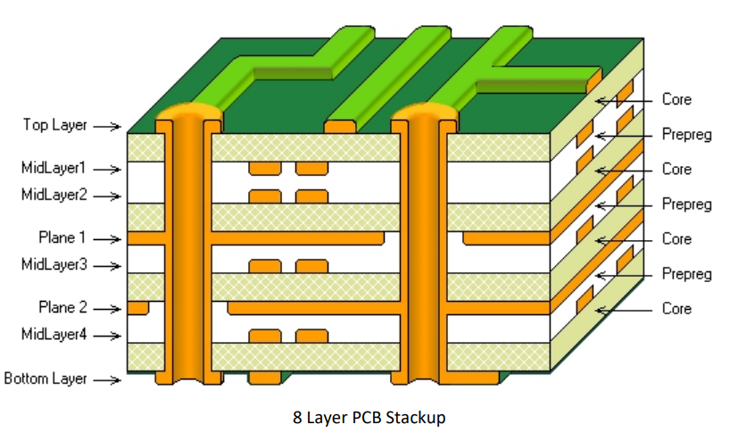
An 8-layer PCB is an increased functionality PCB with a more complex design and higher electromagnetic compatibility (EMC). The plus point of an 8-layer PCB is that it has an adjacent reference and power plane for every signal layer. The adjacent reference planes help in reducing electromagnetic interference (EMI), which ensures high-quality signal transmission.
An 8-layer PCB has two more layers than a 6-layer PCB which can either be used as power planes or for routing signals. If used as power planes, the two additional layers strengthen the circuit's ability to handle high current and decoupling.
What's more? An 8-layer PCB allows mounting more components on a smaller surface. As well as handling mixed signals (analog and digital) on an 8-layer PCB is easier.
In general, A PCB stack-up is the arrangement of the conducting and insulating layers of the PCB. The stack-up design of a PCB is usually done by the PCB engineer or the designer by considering the circuit's requirements. An 8-layer PCB stack-up should at least provide 3 or more power/Ground planes to increase electromagnetic compatibility (EMC is the ability of a circuit or system to work appropriately under electromagnetic interference) and decrease the issues that occur due to EMI.
The planes in the PCB stack-up contribute to isolating the signal layers, which minimize crosstalk among the signals and provide interplane capacitance that helps in rapid switching.
A well-designed PCB stack-up should provide good opportunities to route high-speed, high-frequency and mixed signals. Further, a wisely designed PCB layout can help in reducing the area of the PCB, which somehow relieves the manufacturing cost.
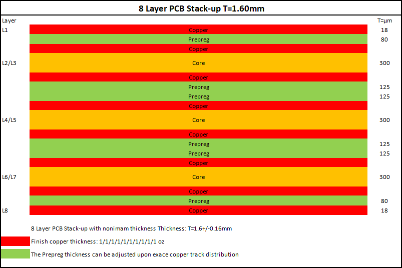
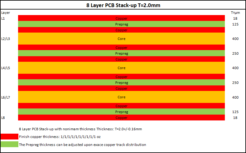
An 8-layer PCB stack-up has 8 conductive (copper) layers separated by 3 layers of core and 4-6 layers of prepregs. The arrangement of these layers in a different manner and with diversified thicknesses of material is given below:

In this stack-up, the number of power planes is reduced to 1 instead of 2, though the number of ground planes is increased to 3, and the power and ground planes are adjacent in the middle of the board. This type of stack-up due to adjacent power planes provides high interplane capacitance, which is necessary to provide rapid switching currents required by the modern logic to operate transmission lines and supply current to the IC cores.
In this stack-up, the number of outermost layers of the Prepreg is doubled. This stack-up is useful when the board requires higher insulation on the outermost signal layers to ensure signal integrity and reduce unnecessary electromagnetic interference (EMI) issues.
This type of stack-up is useful for mixed-signal boards. The outermost layers of this stack-up are adjacent to the ground planes and also have double layers of Prepreg, which provide high shielding to the inner signal layers. Considering this stack-up's configurations, we can route digital signals on the outermost layers and analog in the inner layers to provide maximum shielding and prevent crosstalk among them.

It is not a commonly used stack-up. The ground planes on the outermost layers shield the inner signal layers. This arrangement of the layers is beneficial under circumstances where the environment/surrounding of the board is electrically affected.
Using a pre-designed standard 8-layer PCB stack-up can help you avoid common stack-up mistakes. A standard PCB stack-up also goes well with the manufacturing process because it is a market standard, and fabricators do not need to do anything unusual for which they can charge extra or reject your quote.
The stack-ups we have mentioned above are all standard stack-ups with respect to their widths. However, the arrangement of the layers still depends on the circuit's unique requirements.
The standard thickness of an 8-layer PCB revolves around 1mm to 5mm. Therefore, the thickness of the copper layer, Prepreg and core are important factors to consider while determining the weight and thickness of an 8-layer PCB. At the stage of weight and thickness determination of the PCB, the thickness of different materials is decided by considering the application of the board. For example, if the board has to operate high current, the thickness of the copper layer should be greater than the thickness of the copper layer for a normal board. In simple words, the weight and thickness of an 8-layer PCB are not fixed but depend on different factors.
The sandwich-like structure of a PCB consists of 4 different materials. The copper, Prepreg, core, and solder mask.
Copper is the printed circuit board conducting material, which possesses a network of signal, power, and ground tracks after etching. The standard copper thickness on a PCB is 1.37 mils (1.37 thousandth of an inch). However, the thickness of the copper layer can vary depending on the unique requirements of the board.
The Prepreg is a composite material made up of fibre-glass infused with epoxy resin; it is an uncured OR partially cured material. The main purpose of Prepreg is to bind two layers (either two copper layers or the core and the copper layer) in the PCB and provide the required insulation among the layers. The role of Prepreg in PCB manufacturing is critical.
The solder mask is a liquid epoxy material, mostly green in colour, applied on the outermost layer of the PCB to prevent PCB tracks from oxidation and shorts.
The PCB core is a fully-cured material, which means it is heated and compressed in curing ovens to melt the Prepreg to bind the core with thin copper layers. The PCB core material provides strength to the PCB and is responsible for the various electrical and environmental properties. Such as fire extinguishing, dielectric constant, electromagnetic interference (EMI), etc.
There are different materials used as PCB core. However, the choice of the core material depends on the distinctive requirements of the board.
FR-4 is a glass-reinforced epoxy laminate material and a NEMA grade standard for PCB substrate. The electrical and environmental properties of this material, as well as the cost, make it a perfect substrate for printed circuit boards.
Metal core PCBs use metal as the base material. The advantage of using metal is that metal is a good conductor of heat, so the heat dissipation in metal-core PCBs is exceptional. Further, metal-core PCBs provide great mechanical support.
Ceramic PCBs provide high thermal conductivity, minimal coefficient of thermal expansion (CTE), and stable dielectric constant (DK), which help in minimizing impedance issues.
Composite Epoxy Material is a composite material made up of woven glass fabric surfaces and a non-woven glass core combined with epoxy-synthetic resin. CEM is a family of 5 different base materials. The 3rd material of this family is a common cause of its fame. The properties of CEM-3 are similar to the properties of FR-4, which is the most commonly used base material.
High-frequency laminates are very useful for high-frequency applications. The properties of this laminate eliminate other core materials when signal integrity and impedance are concerned.
In an 8-layer PCB, there is no restriction on using components. We can use any electronic component. Including
Resistors: A resistor is a passive component responsible for controlling the flow of current in a circuit. Another functionality of a resistor is providing constant voltage to active devices, such as transistors.
Diodes: The diodes are responsible for limiting the flow of current in one direction. Different types of diodes have distinct functions. The main uses of diodes are regulating voltage, switching, isolating a signal, etc.
Capacitors: A capacitor is a two-terminal passive component. Whose primary purpose is to store electrical charge. On a double-layer or multilayer printed circuit board, the other uses of a capacitor include power conditioning, signal coupling and decoupling, noise filtering, and remote sensing.
Transistors: The transistors as an 8-layer PCB component can have several applications. Such as regulating current or voltage, amplifying signals, etc. However, the primary purpose of a transistor is to act as a switch or gate for electrical signals.
Sensors: Sensors, as an 8-layer PCB component, sense the changes in the environment and give a pulse to the system according to which the system responds. These changes could be environmental and electrical.
Transformers: In an 8-layer PCB, transformers are used to convert Alternating Current (AC) to Direct Current (DC).
Connectors: The primary function of a connector is to connect the PCB with the actual module or machine and supply power to electrical devices.
LEDs: LEDs emit light when current flow through them. On an 8-layer PCB, LEDs are usually used to notify something special.
On an 8-layer printed circuit board, the arrangement of the signal power and ground planes depends on the requirements of the circuit. But some fundamental rules of electronics should be considered while designing the stack-up.
The arrangement of the layers and planes for a high-speed and high-frequency circuit should be done by considering that every layer should have a ground/power plane adjacent to it. To meet and preserve the electromagnetic compatibility of the 8-layer PCB. Providing adjacent ground and power planes ensures signal integrity and minimizes crosstalk among the signals. What's more? Placing ground and power planes adjacent in the middle of the board (dedicating L-4 for Ground and L-5 for Power) creates interplane capacitance. The interplane capacitance is necessary to provide rapid switching currents, required by the modern logic to operate transmission lines and supply current to the IC cores. The adjacent ground and power planes will also eliminate any possible crosstalk among the L-3 and L-6. So, these layers are ideal for routing signals that require maximum signal integrity.
A mixed-signal PCB refers to a printed circuit board that uses both analog and digital signals. Our above-mentioned 3rd stack-up is an ideal stack-up for mixed circuits. The outermost layers of the 3rd mentioned stack-up are good for routing digital signals as they are adjacent to ground planes and have 2 layers of Prepreg. This arrangement of the planes and signal layer will help in avoiding impedance mismatches, excessive inductance, and radiated noise among the signals. However, the designers can modify the stack-up to increase functionality according to their requirements.
Bottom Line: The arrangement of the layers and planes on an 8-layer printed circuit board has a direct impact on the electromagnetic compatibility and other electrical properties of the board. In an 8-layer PCB, we usually have 2 power and 2 ground planes that can provide maximum shielding to the high-speed and high-frequency signal layers. By modifying the thickness of the core and prepreg materials and with an intelligently designed PCB layout, we can achieve a PCB with high performance.
There are several factors that determine the design of an 8-layer PCB stack-up. Some of them are
The area of the application refers to the domain in which the PCB has to use. The functions of a PCB and its operating environment have a significant impact on the stack-up design of a PCB. As we know, different domains have unique electrical and environmental requirements, so it is necessary to design the stack-up and choose the material accordingly. To meet the distinct specifications of the circuits and achieve the required output, the designers and engineers finalize the stack-up and layout by considering the unique specifications of the circuit board. For a better understanding, let's take it with an example. A circuit operating in a high electromagnetic environment requires high electromagnetic compatibility. While on the other hand, a mixed circuit board demands maximum shielding to avoid crosstalk. These distinct specifications of circuits play a vital role in the determination of the stack-up and layout design of the PCB.
The design configurations of a circuit draw our attention to the hardware details of the printed circuit board. The hardware requirements of the board, such as the thickness and size of the PCB, a pre-defined placement of components, and other specifications, play a vital role in the design determination of the PCB. The design configurations for individual circuits are usually different but crucial to be noted while finalizing the stack-up design. For example, if there is a size limit for the PCB (which is common in PCB reverse engineering), the designers should pay attention to the selection of components, routing of signals, and the number of required layers for the PCB to avoid spacing issues later. Thus, understanding design configuration before deciding on the stack-up and routing tracks is crucial to avoid unwanted issues.
Electrical specifications of a circuit refer to the properties, such as dielectric constant (DK), dielectric breakdown, impedance and coefficient of thermal expansion, etc. The arrangement of the layers, the width of the tracks, the number of vias, and so on affect the electrical properties of the board. To meet these electrical specifications, the circuit should be designed accordingly. Such as for a circuit that requires maximum shielding, keeping outermost layers adjacent to the ground plane provides maximum shielding, signal integrity, and a low dielectric constant. Briefly, understanding the electrical specifications of a circuit is an important factor in determining the stack-up design of an 8-layer PCB.
Due to the complexity of an 8-layer PCB, the designers and manufacturers usually charge more. So, to reduce the manufacturing cost, the engineers try to keep the stack-up and layout design of the PCB as simple and close to the market standard as they could.
Component density refers to the number of components, sizes, and weight. A circuit with high component density will definitely affect the stack-up, maybe in terms of mechanical support or electrical specifications. For example, a circuit with high component density will need more space to make them fit. Further, the PCB will need extra mechanical support to bear the burden of the components. Thus, the core of the PCB will need to be thicker to provide enough mechanical strength to the board. The higher component density can also affect the stack-up design of the board in terms of vias. For example, to place a large number of components on a smaller PCB, the designers will use both sides of the PCB instead of using one. And if the designers use both sides, they will need to connect those layers with blind and buried vias. So, what's the problem with this? Having too many vias in a high-speed circuit can question the signal integrity because vias have inductance.
1. High-speed circuits usually demand interplane capacitance. For example, in an 8-layer PCB achieving interplane capacitance is easy if we put L-4 as a ground plane and L-5 as a power plane. When two planes are adjacent, they create interplane capacitance.
2. In an 8-layer PCB, if you choose to go with 6-signal layers and two planes. Route the signal tracks perpendicular to adjacent signal layers to minimize crosstalk.
3. To avoid noise coupling, induced current and crosstalk in an 8-layer or any-other multilayer PCB keep the Ground planes adjacent to high-speed and high-frequency signal layers to provide maximum shielding to the respected layers.
4. On an 8-layer board, to prevent crosstalk and impedance mismatches, do not route mixed signals on the inner layers of the board unless they are perfectly shielded.
5. On an 8-layer board that is operating under a high electromagnetic environment, try not to route too many vias because vias have inductance, which creates EMI issues.
6. In an 8-layer PCB, if the circuit is operating high current with different voltages, use more than one Power plane. Further, a power plane helps achieve shorter current return paths, which leads to better EMC performance.
The price determination of a 6-layer printed circuit board depends on the three factors
The quality of the material and the thickness of the PCB are the main factors that determine the price of an 8-layer PCB. Therefore, the higher the quality material and PCB thickness you will demand, the higher it will increase the cost.
In some cases, to increase the temperature resistance of the PCB, we need to modify the core material in terms of resin. This modification in the base material burdens the manufacturing budget of the PCB.
The sizes of mounted holes and their dimensions are other factors that affect the manufacturing cost of the board. The greater the quantity of the holes, the more time requires for the manufacturing process. Along with the quantity, the dimensions of the holes matter a lot. Because the smaller holes require more special machinery and time to drill for which, the manufacturers charge more, which eventually end-ups increasing the manufacturing cost of the PCB.
The last but not least point is that some circuits require high-frequency laminates as the substrate instead of standard FR-4 material. Or other substrates based on their individual requirements. Using any other substrate rather than the standard FR-4 can also fluctuate the prices of an 8-layer PCB, maybe at an extreme.
A standard 4-layer PCB provides 2 signal layers, a power plane and a ground plane. On the other hand, a standard 8-layer PCB provides 4 signal layers to route tracks, 2 power planes, and 2 ground planes. In a 4-layer and an 8-layer PCB, the difference not only revolves around the number of layers, but the main difference occurs when it comes to their area of application, cost, and performance.
The 8-layer PCB is higher in performance and durability than the 4-layer PCB. The electromagnetic compatibility of an 8-layer PCB is higher than the 4-layer PCB, which makes it able to provide the required performance under an electromagnetic environment. Due to the increased number of cores and prepregs, the isolating property of an 8-layer PCB is better than a 4-layer PCB. The thickness of an 8-layer PCB is usually more than a 4-layer PCB, which increases the mechanical strength of the PCB. Besides all these properties of an 8-layer PCB, the main thing that matters the most is the stack-up and layout design of the PCB. A well-designed 8-layer PCB stack-up can provide good EMC, interplane capacitance, and maximum shielding to the signal layers, whereas a small mistake on the stack-up side can ruin everything.
In general, the cost of an 8-layer PCB is higher than the price of a 4-layer PCB for an obvious reason. But as we know, several factors determine the cost of the PCB. So, we can't express it in numbers.
The 4-layer and 8-layer PCBs both have different areas of applications. Such as a 4-layer PCB, due to its low cost and good quality, has a wide application in consumer electronics. On the other hand, an 8-layer PCB has applications in more complex areas, for example, in medical and military-grade equipment.
The manufacturing process of an 8-layer PCB includes several steps.
1. The first step of the manufacturing process of an 8-layer PCB is to finalize the stack-up, design the layout on a computer and verify it to omit errors.
2. The second step is to print photo tools/films with the help of laser photo plotters (A type of printer) that take the board's data and convert it into pixeled images. The object of creating these films is to use them later to image the PCBs.
3. The third step is to print the inner layers of the PCB on a laminate which is basically a dielectric material with copper lamination on both sides. To print inner layers, first, the laminate is coated with a photoresist material, then under a UV printer, the laminate is structured in the sandwich form with the pre-made inner films to convert the film's data onto the laminates. After this, the laminates go through a process that removes all the unhardened data from the laminates.
4. The fourth step is to etch or remove the extra copper from the inner layers, which is done by pressure washing the inner layers using an alkaline solution.
5. The fifth step is to punch registration holes into the inner laminates, which will later help us to align inner layers with outer layers.
6. The sixth step is to check if the registration holes are drilled properly and inspect other things as we will not be able to make changes in the inner layers later. This process is done by Automatic Optical Inspection (AOI).
7. The seventh step is to bind the inner layers with Prepreg. This process of different binding layers together is done by the heat pressing method. In this process, the heat melts the epoxy resin, and the high pressure helps layers to stick together.
8. The eighth step is to drill holes for the leaded components and vias to connect copper layers in the PCB. Again, the drilling process is fully computerized to avoid errors.
9. The ninth step consists of electroplating. Electroplating is necessary to deposit some copper on the walls of the holes to make them conductive.
10. The tenth step is to print the outermost layers of the PCB, which is again the same process that has been done for the inner layers.
11. The eleventh step is to electroplate the finalized planes with copper to deposit copper onto the outermost layers of the PCB.
12. The twelfth step is to etch the unwanted copper from the outermost layers by pressure washing the boards using a strongly alkaline solution.
13. The thirteenth step involves the coating of a solder mask. Which is a liquid epoxy material applied on the outermost layers of the PCB to prevent copper from rusting/oxidation.
14. The last step of 8-layer PCB manufacturing is known as silkscreen. Silk Screening is the process of printing information regarding components on the board.
NextPCB is a globally recognized PCB manufacturer, known for delivering high-quality products and exceptional customer service. With over 15 years of experience, we specialize in producing single-layer to multilayer boards. Our expertise and commitment to excellence have positioned NextPCB as one of the leading 8-layer PCB manufacturers worldwide. We produce a wide range of PCB stack-ups, including those listed above and any custom stack-ups provided by our valued clients. Additionally, NextPCB can provide fully assembled and tested 8-layer printed circuit boards, customized to your specific needs.
Our services extend to component sourcing, PCB prototyping, PCB manufacturing, PCB assembly, quality testing, and final shipment. In short, NextPCB is equipped to meet all your PCB needs, from prototyping to both small and large-scale PCB production.
>>Get a quick online PCB quote within 24 hours.
An 8-layer printed circuit board provides enough space to route complex dense circuits with exceptional electromagnetic compatibility (EMC).
The increased number of ground and power planes in an 8-layer PCB provides signal integrity and better opportunities for routing mixed, high-frequency and high-speed signals.
The specifications of an 8-layer board are alone not enough to meet the electrical requirements of the board. Thus, to increase the performance of an 8-layer board, the designers can take different approaches for the stack-up design by considering the unique requirements of the individual boards.
In terms of performance and durability, an 8-layer board is more reliable than the standard 4 and 6-layer boards. Hence, the price of an 8-layer board is also higher than a standard 4 and 6-layer board, which are somehow justifiable.
Still, need help? Contact Us: support@nextpcb.com
Need a PCB or PCBA quote? Quote now


 Surface

