

 NextPCB Capabilities
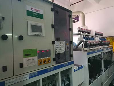
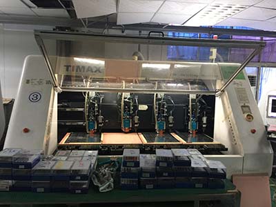
 PCB Assembly
 Layer Buildup
 SMD-Stencils
 PCB Design-Aid & Layout
 Mechanics
 Surface
 Quality
 Drills & Throughplating
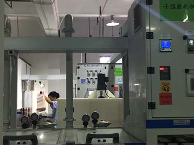
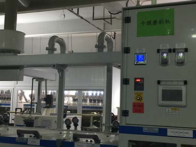
 Factory & Certificate


-

-

-
-
-
-
-

-
-
The sale price for 4-layer PCB!!!!
Good news: A Big Sale on NextPCB, Only $28, you could own 10pcs of 4-layer PCB.
5099 4 0 Shares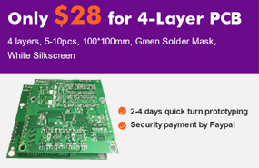
-
-
-
How to use Protel-39 questions and answers
There are 39 questions about how to use Protel-39 and the answers.
6769 4 0 Shares
-
-
-
9 common issues with grounding
9 basic knowledge discussions about grounding technology
7770 9 0 Shares
-
-
-

-
-

Categories
Recommended Article:
- Toroidal vs Drum Core vs Shielded SMD Inductor: Choosing the Right Form Factor
- How to Place Inductors on a PCB: Orientation, Spacing and EMI Rules for DC-DC Converters
- Shielded vs Unshielded Inductors: EMI Impact and PCB Placement Best Practices
- Common Mode Choke: How It Works, PCB Layout Rules and Differential Pair Applications
- Ferrite Bead vs Inductor: When to Use Each for EMI Filtering in PCB Design
- Power Inductor Selection Guide: Inductance, DCR & PCB Footprint
- MLCC Piezoelectric Effect: Acoustic Noise, Microphonics and How to Mitigate in PCB Design
- Bulk vs Decoupling Capacitor: The Three-Tier Capacitor Strategy
- ESR and ESL in Capacitors: What They Mean and Why They Matter in PCB Power Integrity
- Film Capacitor vs Ceramic Capacitor: Applications, Trade-offs and PCB Layout Considerations