

 NextPCB Capabilities
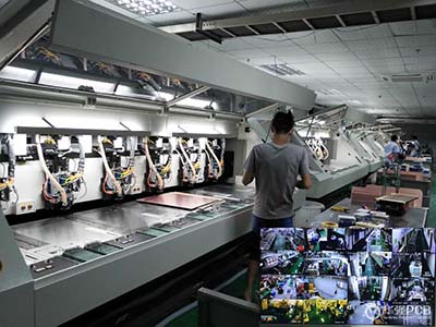
 PCB Assembly
 Layer Buildup
 SMD-Stencils
 PCB Design-Aid & Layout
 Mechanics
 Surface
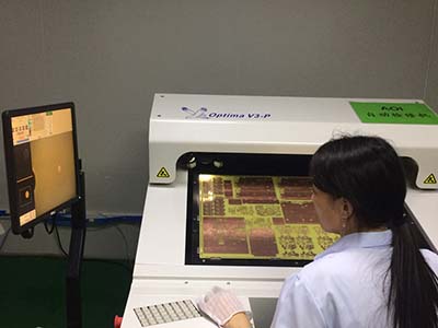
 Quality
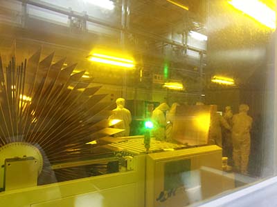
 Drills & Throughplating
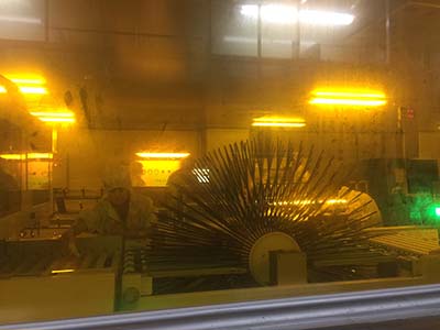
 Factory & Certificate


-

-
-
PCB design tips 100, teach you to master PCB design easily (66-75)
PCB design tips-teach you to master PCB design easily (66-75)
3899 1 0 Shares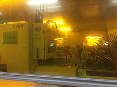
-
PCB design tips 100, teach you to master PCB design easily (56-65)
PCB design tips 100, teach you to master PCB design easily
3733 2 0 Shares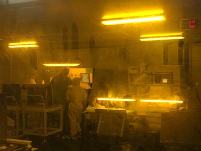
-
PCB design tips 100, teach you to master PCB design easily (46-55)
PCB design tips-teach you to master PCB design easily
3915 1 0 Shares
-
-
-
PCB design tips 100, teach you to master PCB design easily (19-24)
In this article we will teach you how to do a PCB design easily(19-24)
3857 3 0 Shares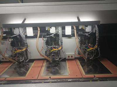
-
PCB design tips 100, teach you to master PCB design easily (11-18)
In the high-speed PCB design, teach your PCB design easily. (11-18)
3947 5 0 Shares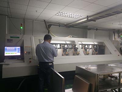
-
-
-

-
India Customer pls provide POA /KYC required
India Customer pls provide POA /KYC required for order PCB in NEXTPCB Manufacturer.
7618 0 0 Shares
-
Freight Discount Promotion Notice
3948 0 0 Shares
-
-
-
CAM350 Basic Steps to Create CAM Data Summary
There are 9 steps to create Cam data by CAM350.
11816 9 0 Shares
-
-
-

Categories
Recommended Article:
- Toroidal vs Drum Core vs Shielded SMD Inductor: Choosing the Right Form Factor
- How to Place Inductors on a PCB: Orientation, Spacing and EMI Rules for DC-DC Converters
- Shielded vs Unshielded Inductors: EMI Impact and PCB Placement Best Practices
- Common Mode Choke: How It Works, PCB Layout Rules and Differential Pair Applications
- Ferrite Bead vs Inductor: When to Use Each for EMI Filtering in PCB Design
- Power Inductor Selection Guide: Inductance, DCR & PCB Footprint
- MLCC Piezoelectric Effect: Acoustic Noise, Microphonics and How to Mitigate in PCB Design
- Bulk vs Decoupling Capacitor: The Three-Tier Capacitor Strategy
- ESR and ESL in Capacitors: What They Mean and Why They Matter in PCB Power Integrity
- Film Capacitor vs Ceramic Capacitor: Applications, Trade-offs and PCB Layout Considerations