PCB Circuit Board Testing, Inspection and Specification (2)
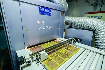
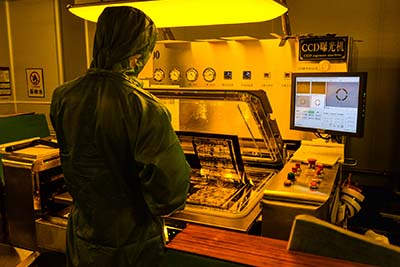
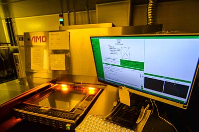
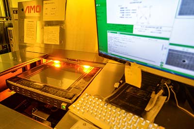
This article provides an in-depth exploration of key terms and techniques in PCB circuit board testing and inspection, covering everything from basic quality control methods to advanced testing technologies. It begins by explaining acceptability and acceptance standards, followed by the application of Acceptable Quality Level (AQL). The article then discusses common defects in PCB manufacturing, such as air inclusion bubbles, blistering, and copper foil warping, and highlights how Automatic Optical Inspection (AOI) and Automatic Testing Equipment (ATE) ensure PCB quality and reliability. Additionally, various quality tests, such as cross-cut tests, continuity tests, and solderability tests, are covered, offering strategies for ensuring that PCBs meet industry standards.
By exploring these testing methods and techniques, the article helps PCB manufacturers and quality control professionals improve production efficiency and maintain high product quality.


 NextPCB Capabilities
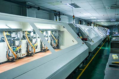
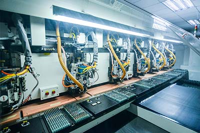
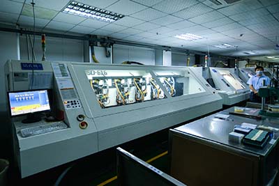
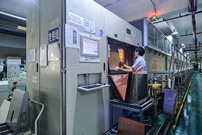
 PCB Assembly
 Layer Buildup
 SMD-Stencils
 PCB Design-Aid & Layout
 Mechanics
 Surface
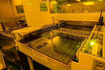
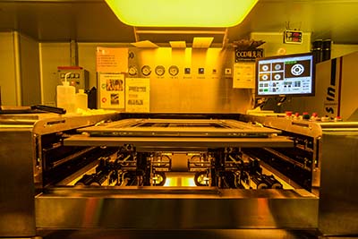
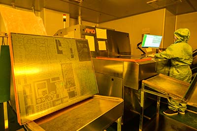
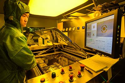
 Quality
 Drills & Throughplating
 Factory & Certificate