
Support Team
Feedback:
support@nextpcb.comEnsure signal integrity:
1. Isolation
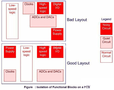
Components on a PCB have various edge rates and various noise differences. The most straightforward way to improve SI is to achieve physical isolation of components on the PCB based on the edge and sensitivity of the device. The figure below is an example. In the example, power supply, digital I/O ports, and high-speed logic are high-risk circuits for clock and data conversion circuits. The clock and data converter placed in the first layout is adjacent to the noise device. Noise will couple to sensitive circuits and reduce their performance. The second layout made effective circuit isolation would be beneficial to the signal integrity of the system design.
2. Impedance, reflection and terminal matching
Impedance control and termination matching are fundamental issues in high speed circuit design. Usually the RF circuit in each circuit design is considered to be the most important part. However, some digital circuit designs with higher frequency than RF ignore the impedance and terminal matching.
Due to the fatal effects of impedance mismatch on digital circuits, see the following figure:
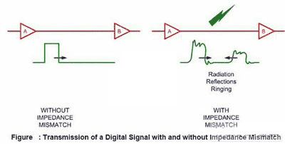
a. The digital signal will cause a reflection between the input of the receiving device and the output of the transmitting device. The reflected signal is bounced back and propagates along both ends of the line until it is finally fully absorbed.
b. The reflected signal causes the ringing effect of the signal through the transmission line, and the ringing will affect the voltage and signal delay and the complete deterioration of the signal.
c. A mismatched signal path can cause the signal to radiate to the environment.
Problems caused by impedance mismatch can be minimized by terminating resistors. The terminating resistor is usually placed on one or two discrete devices on the signal line close to the receiving end. The simple method is to connect small resistors in series.
The terminating resistor limits the signal rise time and absorbs some of the reflected energy. It is worth noting that the use of impedance matching does not completely eliminate the destructive factors. However, careful selection of the appropriate device, terminal impedance can be very effective in controlling signal integrity.
Not all signal lines require impedance control, such as characteristic impedance and termination impedance characteristics in requirements such as compact PCI specifications.
For other standards that do not have the requirements of the impedance control specification and the designer did not pay special attention to it. The final standard may change from one application to another. Therefore, it is necessary to consider the length of the signal line (correlation and delay Td) and the signal rise time (Tr). The general rule for impedance control is that Td (delay) should be greater than 1/6 of Tr.
3. Internal and internal electrical layer division
Factors that are ignored by digital circuit designers in current loop design include considerations for the transmission of single-ended signals between two gates (see the figure below). The current loop from gate A to gate B is then returned from ground plane to gate A.
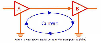
There are two potential problems in the picture above:
a) The ground plane between the two points A and B needs to be connected through a low impedance path. If a large impedance is connected between the ground planes, voltage backflow will occur between the ground plane pins. This will inevitably result in distortion of the signal amplitude of all devices and superimpose the input noise.
b) The area of the current return loop should be as small as possible, and the loop is better than the antenna. Usually speaking, a larger loop area will increase the chance of loop radiation and conduction. Every circuit designer wants the return current to be directly along the signal line, thus the smallest loop area.
Using a large area of grounding can solve both problems at the same time. Large area grounding provides a small impedance across all ground points while allowing the return current to return directly along the signal line as much as possible.
A common mistake in PCB designers is to make holes and slots in the geoelectric layer. The figure below shows the current flow as a signal line on a grounded geoelectric layer. The loop current will be forced to bypass the slot, which inevitably creates a large loop loop.
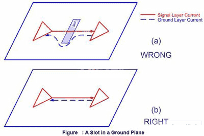
In general, it is not possible to slot on the ground power plane. However, in some cases where it is inevitable to slot, the PCB designer must first determine that no signal loops have passed through the slotted area. The same rules apply to mixed signal circuits.
No multiple layers are used in the PCB. In particular, in high-performance ADC circuits, it is possible to effectively reduce the interference between signals by using a ground layer that separates analog signals, digital signals, and clock circuits. Need to emphasize again, in some cases where it is inevitable to slot, the PCB designer must first determine that there is no signal loop in the slotted area.
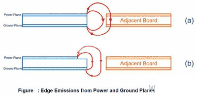
Also pay attention to the area of the interlayer area in the power plane with a mirror difference (as shown below). There is a radiation effect of the power plane layer on the ground plane layer at the edge of the board. Electromagnetic energy leaking from the edge will destroy adjacent boards. See picture a below. Properly reduce the area of the power plane layer (see Figure b below) so that the ground planes overlap in a certain area. This will reduce the impact of electromagnetic leakage on adjacent boards.
4. Signal wiring
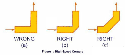
The most important to ensure signal integrity is the physical routing of the signal lines. PCB designers are often under working pressure, not only to complete the design in the shortest possible time, but also to ensure signal integrity requirements. Mastering how to balance the problems that may arise with the spacing of the signals will drive the process of system design. High speed currents do not effectively handle discontinuities in the signal line. The problem of signal discontinuity is most likely to occur in the following figure a. In low-speed circuits, there is usually no need to consider signal discontinuities, and this problem must be considered in high-speed circuits. Therefore, the continuity of the signal can be effectively ensured in the circuit design and in the manner shown by b/c in the following figure.
Another common problem with signal routing in high-speed circuit design. If there are no special reasons, all short wires should be eliminated as much as possible. In high-frequency circuit design, the short wiring is the same as the radiation caused by the impedance matching of the signal lines.
In the wiring of high-speed circuit design, special attention should be paid to the wiring of differential pairs. The differential pair is driven by two fully complementary signal lines. Differential pairs are good for avoiding noise interference and improving S/N rates. However, differential pair signal line pairs have particularly high requirements:
1. The two wires must be as close as possible to the wiring;
2. The two lines must be exactly the same length;
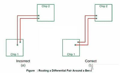
Routing a differential pair of signal lines between two devices that are not aligned together is a critical issue.
In the above picture a, there are some uncertainties due to the inconsistent length of the two signal lines. The correct wiring should be in the manner shown in Figure b above. The general rule in differential pair routing is to keep the two signal lines equally spaced and close to each other.
5. Crosstalk
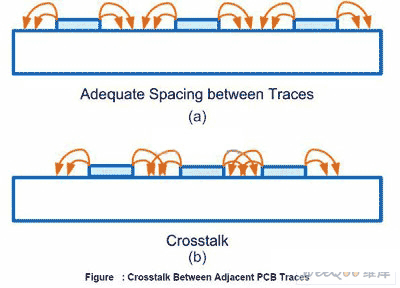
Crosstalk is another concern in PCB design. The following figure shows the crosstalk area between adjacent three pairs of side-by-side signal lines in a PCB and the associated electromagnetic area. When the interval between the signal lines is too small, the electromagnetic regions between the signal lines will affect each other, resulting in deterioration of the signal, which is crosstalk.
Crosstalk can be solved by increasing the signal line spacing. However, PCB designers are often constrained by increasingly tight wiring spaces and narrow signal line spacing; as there are no more options in the design, it is inevitable to introduce some crosstalk problems into the design. Clearly, PCB designers need some ability to manage crosstalk problems. There are many rules for reliable spacing in these years. A commonly accepted rule is the 3W rule, that is, the spacing of adjacent signal lines should be at least three times the width of the signal line. However, the actual acceptable signal line spacing depends on factors such as the actual application, the working environment, and design redundancy. The signal line spacing is changed from one situation to another and each calculation. Therefore, when crosstalk problems are unavoidable, crosstalk should be quantified. This can be expressed by computer simulation techniques. With the simulator, the designer can determine the signal integrity effects and the crosstalk effects of the system.
6. Power supply decoupling
Power decoupling is now a standard practice in digital circuit design, and the mention here will help reduce noise problems on the power line. A clean power supply is critical to designing a high performance circuit. The high frequency noise superimposed on the power supply will cause problems for each adjacent digital device. Typical noise is derived from ground bounce, signal radiation, or the digital device itself. The easiest way to solve power supply noise is to use a capacitor to decouple high frequency noise from the ground. The ideal decoupling capacitor provides a low-impedance path to ground for high-frequency noise, eliminating power supply noise. Depending on the application, decoupling capacitors are chosen. Most designers will choose surface-mount capacitors as close as possible to the power supply pins, and the capacitance should be large enough to provide a low-impedance path to the foreseeable power supply noise. A common problem with decoupling capacitors is that the decoupling capacitor cannot be simply used as a capacitor. There are several situations:
a. The capacitor package will lead to parasitic inductance;
b. The capacitor will bring some equivalent resistance;
c. The wire between the power supply pin and the decoupling capacitor will bring some equivalent inductance;
d. The wire between the ground pin and the ground plane will bring some equivalent inductance; the resulting effect:
a. The capacitor will induce a resonance effect on a specific frequency and the network impedance generated by it will have a greater influence on the signal of the adjacent frequency band;
b. The equivalent resistance (ESR) will also affect the low resistance path formed by high speed noise decoupling;
The following summarizes the resulting effects on a digital designer:
a. The leads from the Vcc and GND pins on the device need to be treated as small inductors. It is therefore recommended to make the leads of Vcc and GND as short and thick as possible in the design.
b. Select a capacitor with a low ESR effect, which helps to improve the decoupling of the power supply;
c. Choosing a small package capacitor device will reduce the package inductance. Changing the device in a smaller package will result in a change in temperature characteristics. Therefore, after selecting a small package capacitor, you need to adjust the layout of the device in the design.
In the design, replacing the capacitors of the X7R model with Y5V capacitors ensures a smaller package and lower equivalent inductance, but at the same time it costs more to ensure high temperature characteristics.
Decoupling of low frequency noise with bulk capacitors should also be considered in the design. The use of separate electrolytic capacitors and tantalum capacitors can greatly improve the cost performance of the device.
7. Summary:
Signal integrity is one of the most important issues throughout high-speed digital circuit design; here are some suggestions for ensuring signal integrity in digital circuit design:
a. Perform physical isolation of the noise device on the sensitive component;
b. Impedance control, reflection and signal terminal matching;
c. Using a continuous power supply and ground plane;
d. Avoid using right angles in the wiring;
e. The differential pair wiring length is equal;
f. The crosstalk problem should be considered in the design of high speed circuits;
g. Power supply decoupling problem.
Still, need help? Contact Us: support@nextpcb.com
Need a PCB or PCBA quote? Quote now