
 NextPCB Capabilities
Printed Circuit Boards
NextPCB Capabilities
Printed Circuit Boards
 PCB Assembly
 Layer Buildup
 SMD-Stencils
 PCB Design-Aid & Layout
 Mechanics
 Quality
 Drills & Throughplating
 Factory & Certificate
 PCB Assembly Factory Show
Certificate
PCB Assembly Factory Show
Certificate
Support Team
Feedback:
support@nextpcb.com


Component density refers to the quantity of transistors per chip in digital integrated circuits (ICs). It continues to grow yearly. The physical volumes of individual atoms place a practical limit on component density, despite some engineers' predictions that they will be able to have a single atom perform numerous functions.
The atomic structure of semiconductor material imposes an absolute limit on the component density that can be achieved. There will never be a logic gate created that is smaller than a single atom. The barrier has not yet been crossed by technology. We discuss in detail component density and different metrics to check component density.
We need to determine the necessary densities and then compare alternative board construction techniques to get the most affordable design which are crucial for the proper design of PWBs. You should know there are several fundamental phrases, terminologies, and formulas for calculating and analyzing the wiring density of PWBs.
To determining the necessary wire density, till now, several engineers empirically develop different equations that allow calculating the demand for such wiring.
$$W_c=\frac{T*L}{G}\ in/in^2$$
Let's explain PWB equation formula in detail:
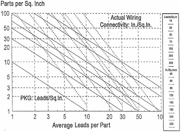
Determining the necessary wire density, however, which will be adequate to link all the components on the chosen board size, is more crucial. We use a number of equations to calculate such wire demands. But, dr. D. Seraphim creates the simplest version, which is:
Wd = 1.25NtP
Where,
To analyse and make the relationships between component density and PWB density, proficient engineers develop number of metrics. This is because the parts and their terminations have a significant impact on the design of the PWB. H. Holden has managed a complete analysis of these relationships.
You can use this information to predict the predicted PWB density and where the suggested product will fall on the component density spectrum.
In order to handle the chosen level of component difficulty, we would like to explain the Figure. 3 that shows the relationships between the density of the parts, the density of their terminals, and the required wire density. The wire connectivity definition of Wf is given.
We will examine the special metrics as uncased or bare chip assembly on substrates has gained popularity primarily as a result of its capacity to reduce the amount of interconnections. This assembly's optimal boundary would be where all of the chips packed closely together with no gaps.
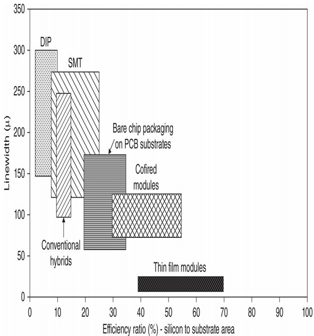
The packaging efficiency would be 100% as counted by the ratio of silicon area to substrate area as a result. This metric is useful for ranking different substrate construction or bare chip attachment methods, as shown in Fig. 4, even though it is obviously not possible to achieve such 100% capability.
Achieving 100% packaging efficiency is impossible since all chip-mounting techniques require some amount of space around the chips. Even when using flip chips, you need to sure that there must still be enough space between the chips for the positioning tool.
| Attachment Method | Chip Spacing, mils |
|---|---|
| Flip-chip | 15-20 |
| Wire-bonding | 70-80 |
| Flip TAB | 100-120 |
| Regular TAB | 150-400 |
The importance for the required distance between the chips (or the total width of the frame around the chips) for various chip bonding techniques are provided in Table. 1 by Dr. H. Charles of Johns Hopkins University. Several other sources have also mentioned these distances or ones that are extremely comparable to them.
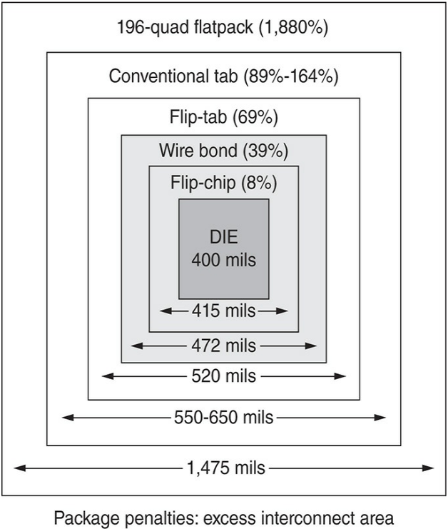
Packaging efficiency must be reduced to around 90% even with flip-chip mounting, to 70% for wire-bonding, and to roughly 50% for TABs, and in certain cases even more. Figure. 5 depicts a situation that is similar. The wiring bond pads on each part are the only ones that should always accommodate the packaging efficiency de-ratings, as we can see in Fig. 5 However, mounting bare chips on PWBs compels more signal spread in the space, permitting for the further installation of larger-diameter PTHs for interfacing with internal layers.
Except for the fact that we can use and mount parts on both sides of the PWB substrate. And it is obvious that direct chip bonds on PWBs will surely reduce the packaging efficiency of such assemblies. With some unique changes, the picture shows that wire-bonding and outer lead bonding (OLB) of TABs are able to carry out on both sides of the PWB. As a result, while single-sided bare chip assembly on PWBs reduces its package efficiency to roughly half that of other parts constructions, the capability to insert components on both sides of PWBs raises it back to the same level as other parts constructions.
In this article, we explore everything related to the component density and its relationship with PWB with different examples and formulas. If you want any more information regarding the topic let us know in the comment section.
Still, need help? Contact Us: support@nextpcb.com
Need a PCB or PCBA quote? Quote now


 Surface

