
 Surface


Lolly Zheng- Sales Account Manager at NextPCB.com

 NextPCB Capabilities
Printed Circuit Boards
NextPCB Capabilities
Printed Circuit Boards
 PCB Assembly
 Layer Buildup
 SMD-Stencils
 PCB Design-Aid & Layout
 Mechanics
 Quality
 Drills & Throughplating
 Factory & Certificate
 PCB Assembly Factory Show
Certificate
PCB Assembly Factory Show
Certificate
Support Team
Feedback:
support@nextpcb.com


Modern electric vehicles (EVs) and autonomous driving systems demand highly reliable, specialized circuit boards. Automotive PCBs must withstand severe thermal cycling, mechanical vibration, and moisture while handling high currents (BMS) or high-frequency signals (mmWave radar). Designing and manufacturing these boards requires strict adherence to IATF 16949 and IPC-6012DA standards. Selecting the right substrate (High-Tg FR4, PTFE, Ceramic, or Metal Core) and leveraging advanced PCB manufacturing techniques like HDI and rigid-flex are non-negotiable for automotive electronic control units (ECUs).
Automotive circuit boards serve as the central nervous system for central control units, ignition systems, powertrain controllers, and Advanced Driver Assistance Systems (ADAS). Unlike standard consumer electronics, automotive electronic hardware lacks a single unified architecture; instead, it relies on highly specialized, customized modules engineered for absolute reliability.
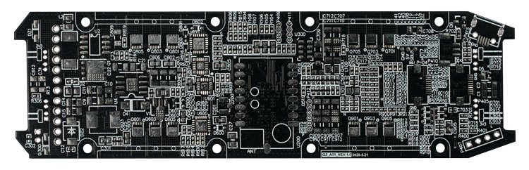
A typical automotive-grade ECU (Electronic Control Unit) mainboard featuring a high-density layout and specialized black finish for improved thermal radiation and inspection contrast.
The transition from internal combustion engines (ICE) to hybrid and pure electric vehicles (EVs) has drastically increased the volume and complexity of automotive PCBs. EV electronics dictate stringent requirements for high-voltage conversion (DC-DC converters, inverters) and Battery Management Systems (BMS). Similarly, intelligent driving systems heavily rely on mmWave radar, requiring specialized low-loss PCB materials. Sourcing from certified automotive PCB manufacturers ensures your designs meet these aggressive performance and safety metrics.
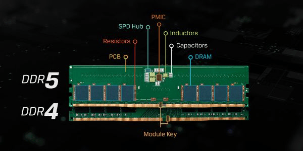
The transition from DDR4 to DDR5 in automotive infotainment systems. Note the integration of the PMIC directly onto the PCB for more efficient power management.
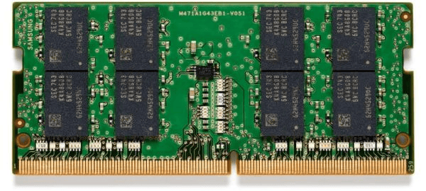
High-reliability automotive DRAM module designed to withstand wide temperature fluctuations in vehicle cockpits.
HDI technology addresses the miniaturization requirements of automotive infotainment and ADAS modules. IPC standards define HDI by the utilization of microvias (vias with a diameter ≤ 150μm). These microvias connect adjacent copper layers without penetrating the entire board substrate, significantly increasing routing density.
Manufacturing HDI boards requires laser drilling and sequential build-up techniques. A via connecting internal layers exclusively is a buried via, while a via connecting an outer layer to an internal layer is a blind via. Typical automotive HDI parameters push track widths below 0.1mm and pad diameters below 0.25mm. This extreme density allows engineers to route complex BGA packages commonly used in automotive microcontrollers.
Rigid-flex boards integrate polyimide (PI) flexible substrates with standard rigid laminates (like FR4), enabling 3D assembly in space-constrained vehicle areas. They provide the mechanical stability of a rigid board where components are mounted, coupled with the dynamic or static bending capabilities of a flexible circuit.
Automotive applications, such as steering column electronics, transmission sensors, and radar modules, rely on rigid-flex structures to eliminate wire harnesses and mechanical connectors. This integration reduces weight and eliminates common points of mechanical failure. Complex rigid-flex stackups can exceed 20 layers, requiring precise impedance control and advanced PCB assembly techniques.
FPCs consist of a flexible dielectric base (usually polyimide), metallic conductor foils, and protective coverlays. Their primary advantage lies in their ultra-thin profile (typically 0.06mm to 0.3mm) and dynamic bending endurance. FPCs replace bulky wiring harnesses in tight enclosures, such as battery pack voltage monitoring lines and automotive display clusters.
LED lighting in modern vehicles—ranging from high-beam headlamps to interior ambient lighting—generates significant thermal loads. Standard FR4 substrates degrade rapidly under these conditions. Metal Core PCBs (MCPCBs), utilizing an aluminum or copper backing, provide a highly efficient thermal path to dissipate heat away from the LED junctions, extending component lifespan and maintaining luminous efficacy.
Selecting the correct base material dictates the thermal, electrical, and mechanical boundaries of the printed circuit board. Automotive environments often exceed the operating limits of standard FR4 (Tg 130℃), necessitating advanced substrate engineering.
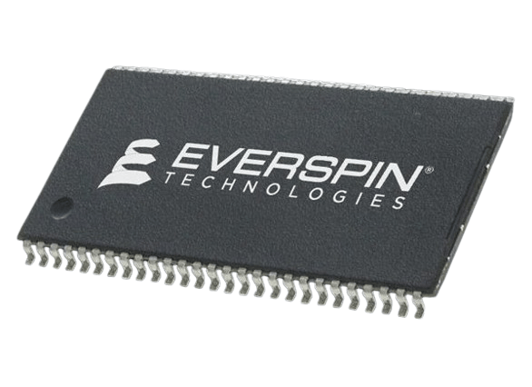
Non-volatile memory solutions like MRAM are increasingly used in automotive black boxes (EDR) due to their high endurance and fast write speeds.
Standard PCBs utilize 1oz or 2oz copper foil. EV powertrains, DC-DC converters, and BMS units require heavy copper PCBs (ranging from 3oz to 10oz+) to manage extreme current loads without catastrophic thermal runaway. The manufacturing process relies on controlled electroplating. Engineers must calculate trace widths accurately, as etching thick copper induces a trapezoidal cross-section due to lateral etching. For instance, etching a 50μm foil results in a larger width tolerance than a standard 18μm foil, demanding specific DFM compensation rules.
Advanced collision avoidance and autonomous driving rely on 77GHz mmWave radar systems. Standard epoxy resins exhibit high dielectric loss (Df) at these frequencies, absorbing the radar signal. PTFE-based laminates (such as the Rogers 3000 or 4000 series) mixed with ceramic fillers offer exceptionally low Df and stable Dielectric Constant (Dk) across wide temperature variations, making them the industry standard for automotive RF applications.
For under-the-hood applications exposed to extreme ambient temperatures, ceramic substrates (like Alumina Al2O3 or Aluminum Nitride AlN) offer unmatched thermal conductivity and a Coefficient of Thermal Expansion (CTE) that closely matches bare semiconductor dies. Ceramic boards are predominantly used in high-power IGBT modules and bare-die wire bonding applications.
Automotive PCBs face relentless environmental stress. Micro-cracking in vias, trace delamination, and substrate degradation can trigger complete system failures. Industry-standard reliability tests simulate decades of vehicle operation in controlled laboratory environments.
>> Recommend reading: Automotive PCB Design: IPC-6012DA, AEC-Q200 and What Makes Car-Grade Boards Different
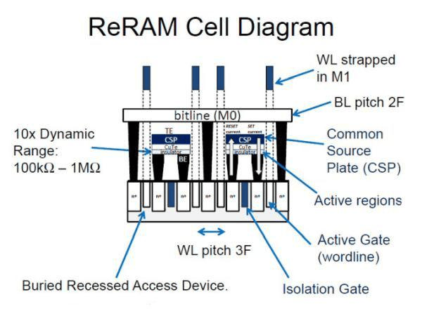
Cross-sectional diagram of a ReRAM cell. This emerging technology is being evaluated for next-generation automotive AI processors due to its low power consumption.
Reputable manufacturing facilities strictly adhere to the following protocols:
A flawless schematic means nothing if the board cannot be reliably manufactured or assembled. Applying Design for Manufacturing (DFM) principles early prevents costly redesigns and accelerates your quick turn PCB prototyping cycles.
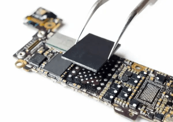
Precise BGA component placement. Automotive PCBA requires extreme accuracy in pad registration to ensure long-term solder joint reliability under vibration.
The global automotive PCB market continues to outpace general electronics growth, driven by EV adoption and autonomous technologies. Securing a reliable supply chain is critical for automotive hardware teams. NextPCB operates advanced manufacturing facilities tailored for new energy vehicle electronics, deploying sophisticated R&D equipment and stringent quality controls.
Whether you need a low cost PCB for an initial prototype or high-volume production for a Tier 1 supplier, NextPCB delivers comprehensive capabilities (1-32 layers), including:
NextPCB provides a true turnkey PCB solution with our Custom Automotive PCB Assembly Service. We handle everything from bare board fabrication to component sourcing and final assembly. Our PCBA capabilities cover:
From single-board engineering prototypes to continuous medium-scale production runs, partner with NextPCB to accelerate your automotive hardware deployment.
Most modern ECUs require at least a 4-layer or 6-layer PCB stackup. This allows engineers to dedicate internal layers exclusively to solid ground and power planes, which provides essential EMI shielding and thermal dissipation required for high-frequency switching and microcontroller stability.
Automotive PCBs undergo aggressive accelerated life testing to simulate 15+ years of driving conditions. Primary tests include:
Heavy copper PCBs are mandatory in EVs to handle massive electrical currents without overheating. By utilizing copper weights between 3oz and 10oz, these boards efficiently distribute current in Battery Management Systems (BMS) and DC-DC power inverters, mitigating the risk of thermal runaway and trace degradation.
IPC Class 3 and the automotive-specific IPC-6012DA mandate stricter manufacturing tolerances compared to Class 2 consumer electronics. They require thicker through-hole copper plating (minimum 25μm), zero tolerance for annular ring breakout, and stricter limits on internal voiding, ensuring absolute reliability in life-critical automotive systems.

Still, need help? Contact Us: support@nextpcb.com
Need a PCB or PCBA quote? Quote now

