
 NextPCB Capabilities
Printed Circuit Boards
NextPCB Capabilities
Printed Circuit Boards
 PCB Assembly
 Layer Buildup
 SMD-Stencils
 PCB Design-Aid & Layout
 Mechanics
 Quality
 Drills & Throughplating
 Factory & Certificate
 PCB Assembly Factory Show
Certificate
PCB Assembly Factory Show
Certificate
Support Team
Feedback:
support@nextpcb.com


In PCB design, many places need to consider safe spacing, including wire spacing, character spacing, pad spacing, and so on. Here, it is temporarily classified into two categories: one is electrically-related safety spacing, and the other is non-electrically-related safety spacing.
As far as the processing capability of the mainstream PCB manufacturer is concerned, the spacing between the wires shall not be less than 0.075 mm. Minimum line spacing, the minimum spacing between fingerboard line to line, line to pad. From a production point of view, the larger the line spacing, the more common is 0.25 mm.
As far as the machining capacity of the mainstream PCB manufacturer is concerned, the solder pad is. For the mechanical drills, the pad aperture shall have a minimum diameter of 0.2 mm. In the laser drilling, the aperture shall be at least 0.1 mm. The aperture tolerance varies slightly according to different plates. Generally, it can be controlled within 0.05 mm, and the minimum width of the pad should not be less than 0.2 mm.
The spacing between pads shall not be less than 0.2 mm as far as the processing capacity of mainstream PCB manufacturers is concerned.
The distance between the live copper skin and the PCB board edge should be no less than 0.3 mm. You can set this spacing rule on the Design>>Rules>>Design Rule window in Altium.
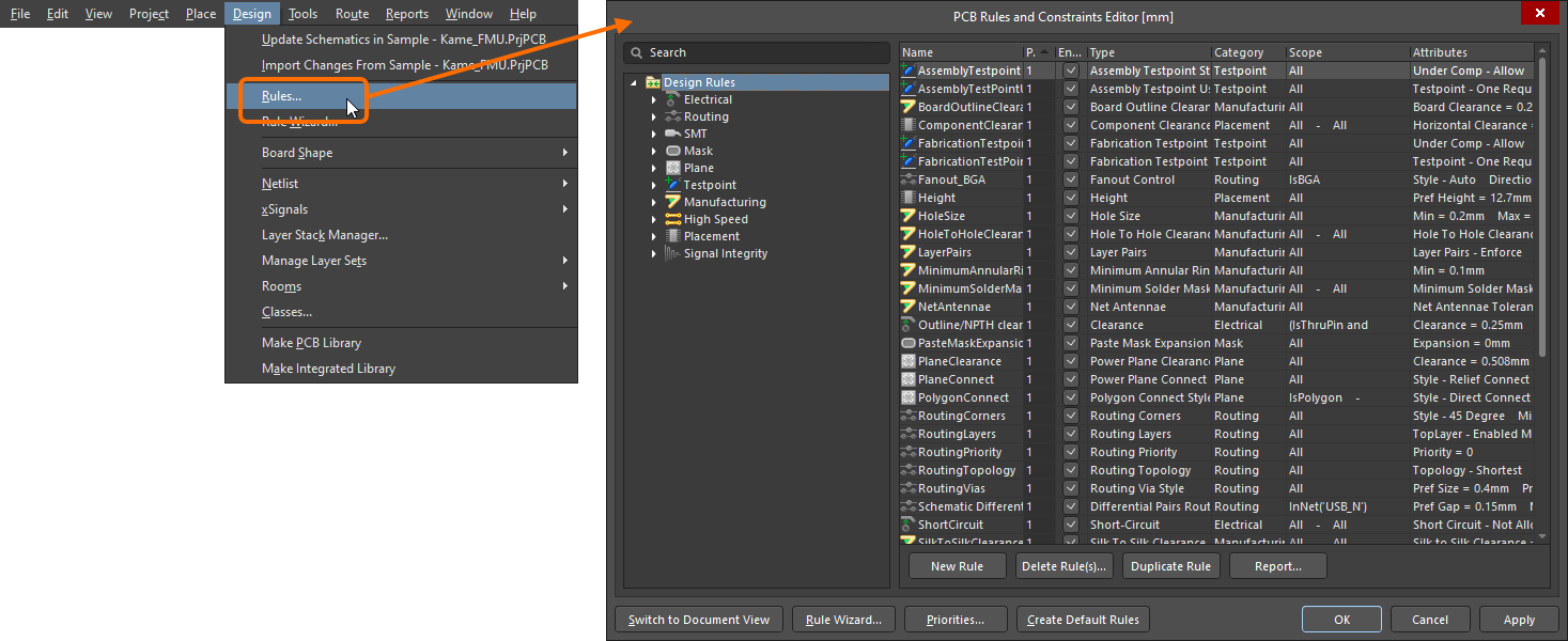
If it is a large area of copper, usually the plate edge needs to have an indented distance, generally set to 0.5 mm. Generally, engineers often shrink the large area of copper coating to the edge of the board by 20 mil, rather than the copper coating to the edge of the board all the time. Because of mechanical considerations of the finished circuit board, or to avoid the occurrence of curling or electrical short circuit caused by the exposure of copper skin on the edge of the board,
There are many ways to handle this copper indenting, such as drawing a keepout layer on the edge of the plate and setting the distance between the copper and the keepout. Here we introduce a simple method: setting different safety spacing for the copper coating object, for example, the safety spacing of the whole board is set to 0.25 mm, and the copper coating is set to 0.5 mm, which can achieve the effect of 0.5 mm inside the edge of the plate. And also remove the dead copper (floating copper island) that may appear in the device.
No changes can be made during the processing of text film, except that the line width of characters with D-CODE less than 0.22 mm (8.66 mil) is enlarged to 0.22 mm, that is, the line width of characters L = 0.22 mm (8.66 mil). The width of the whole character W = 1.0 mm, the height of the whole character H = 1.2 mm, and the spacing between the characters D = 0.2 mm. When the text is less than the above standard, the processing printing will be blurred.
Through-hole (VIA) to through-hole spacing (hole to hole side) should be greater than 8mil.
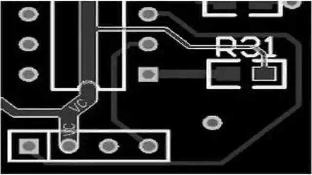
Silkscreen is not allowed to cover the pad. Because the silkscreen will not be tin when tin, thus affecting the installation of components. Generally, the PCB manufacturer requires a spacing of 8 mil to be reserved. If the circuit board is limited in area, the spacing of 4 mil is also acceptable. If the silkscreen is accidentally over the pad during the design, the PCB manufacturer will automatically eliminate the screen part left on the pad during manufacturing to ensure the tin is on the pad.
But the design on a case-by-case basis. Sometimes the silkscreen is deliberately close to the pad because when two pads are very close, the middle screen printing can effectively prevent the short circuit of the solder connection during welding, which is another case.
When assembling PCB components, it is necessary to consider whether there will be conflicts with other mechanical structures in the horizontal direction and spatial height. Therefore, in the design, the compatibility between components, PCB, shell, and spatial structure should be fully considered. And safe spacing should be reserved for each target object to ensure that no conflicts occur in space.
The above data are only for reference, which is convenient to have a direction when designing the safety value, and do not completely represent the industry standard. NextPCB provides 1~32 layer PCB manufacturing services, high reliability, and short delivery time! NextPCB strictly implements the IPC-2 standard, that is, the average hole copper thickness of the shipped circuit board is ≥20 μm. If you require PCB board production, please feel free to request an online PCB quote.
Still, need help? Contact Us: support@nextpcb.com
Need a PCB or PCBA quote? Quote now


 Surface

