PCB Assembly
Lolly Zheng- Sales Account Manager at NextPCB.com

 NextPCB Capabilities
Printed Circuit Boards
 Process Capabilities
 PCB Design-Aid & Layout
 Quality
 Drills & Throughplating
 Factory & Certificate
 PCB Assembly Factory Show
Certificate

Support Team
Feedback:
support@nextpcb.com


Wave soldering and reflow soldering are the two mainstream ways to solder a PCB assembly. Reflow melts solder paste that was printed onto the pads and is the standard process for surface-mount (SMT) components. Wave soldering passes the underside of the board over a pumped wave of molten solder and is used mainly for through-hole (THT) components. Many real-world boards need both, so the real question is usually not "which is better" but "which process fits my board, volume and budget."
Quick answer
Table of Contents
| Reflow soldering | Wave soldering | |
|---|---|---|
| Best for | SMT parts: chip components, QFN, BGA, fine-pitch ICs | Through-hole leads and connectors, especially in larger batches |
| Solder source | Solder paste printed through a stencil | Molten solder in a pot, pumped into a wave |
| Flux | Already inside the paste | Applied separately (spray or foam) before preheat |
| How heat is applied | Whole board heated in a multi-zone oven following a temperature profile | Board is preheated, then the bottom side contacts the wave for a few seconds |
| Typical temperatures | Peak about 235–250 °C for SAC305 lead-free paste (follow the paste datasheet) | Solder pot roughly 250–265 °C for lead-free alloys; contact time about 2–5 seconds |
| Equipment | Stencil, pick-and-place machine, reflow oven | Fluxer, preheater, solder pot, usually pallets or fixtures |
| Typical defects | Tombstoning, voids, head-in-pillow, solder balls, bridging | Bridging, solder skips, icicles, insufficient hole fill |
| Inspection | SPI, AOI, and X-ray for hidden joints | AOI, visual inspection, functional test |
Reflow soldering joins SMT components by melting solder paste that has been printed on the PCB pads. After the components are placed on the paste, the whole board travels through a multi-zone oven. The paste melts, wets the pads and component terminations, and solidifies into joints as the board cools. No mechanical pressure is needed. The temperature profile does the work.
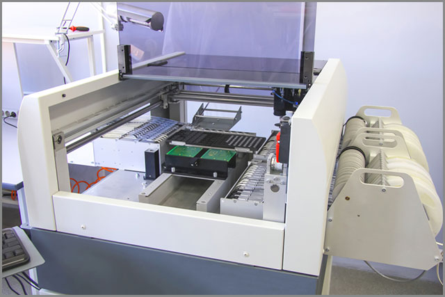
Reflow is the default for SMT because it handles tiny parts and dense layouts that a wave cannot reach. Through-hole parts are normally added afterwards with wave or selective soldering. For a deeper definition, see our reflow soldering glossary entry.
For BGA and QFN packages the joints are hidden under the body, so watch for voids and head-in-pillow defects and verify with X-ray inspection.
Reflow quality also depends on paste deposition. Stencil thickness and aperture design directly affect bridging and insufficient solder, which is why fine-pitch boards need a well-specified SMT stencil.
Wave soldering is a bulk soldering process for through-hole components. The leads are inserted from the top, and the board's underside is passed over a standing wave of molten solder that fills the plated holes and forms all the joints in a single pass. It uses no solder paste; the solder comes directly from the molten bath. In some regions, especially in Japan, wave soldering is also called "flow soldering," so "flow soldering vs reflow soldering" is the same comparison.
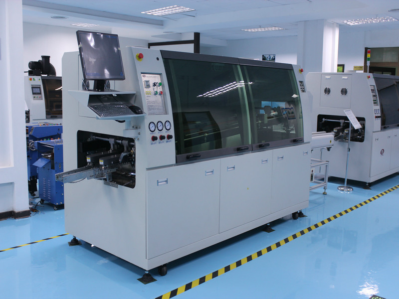
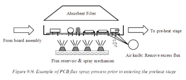
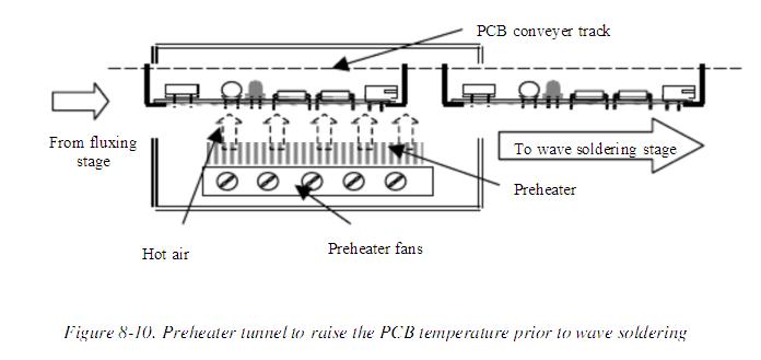
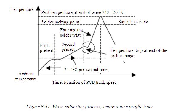
We keep this section short on purpose. For parameters, machine types and troubleshooting, read our full wave soldering process guide.
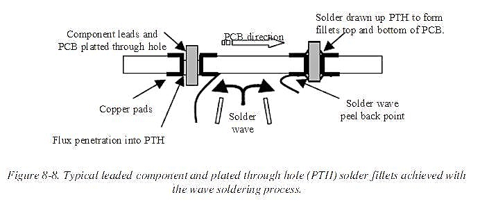
Its limits: it solders the bottom side only, it cannot handle fine-pitch or bottom-terminated packages, and it exposes the board to more thermal stress than selective methods.
Yes, but only in limited cases. Small SMD parts (chip resistors and capacitors, some SOT and SOIC packages) can be glued to the bottom side with an adhesive dot, cured, and then carried over the wave together with the through-hole leads. This was common in older mixed-technology designs.
Be careful with these constraints:
For most modern designs, the better approach is to reflow all SMD parts and solder the through-hole parts with selective soldering, or use pin-in-paste (paste printed into the holes so suitable through-hole parts go through the reflow oven).
Reflow works for nearly every SMT package, including BGA, QFN and 01005 parts. Wave works for through-hole leads and a narrow set of glued SMD parts. Many connectors and electrolytic capacitors cannot tolerate a full pass through the reflow oven, which is why through-hole parts are usually soldered as a separate step.
Neither process is cheaper in every case. SMT-only boards are naturally reflowed because paste printing and placement are needed anyway. For through-hole-heavy boards in volume, wave soldering lowers the cost per joint. For small batches, the pallets, fixtures and machine setup can outweigh that benefit, and selective or hand soldering may cost less overall.
A wave line is continuous and very fast for through-hole joints. Reflow throughput depends on the whole sequence of printing, placement and oven time, and it is the most efficient route for dense SMT designs.
Reflow heats the entire assembly with a controlled profile. Wave soldering hits the bottom side with molten solder, so bottom-side parts and the laminate see a sharper thermal event. Pad shape, spacing and component orientation matter more for wave than for reflow.
Neither method is inherently more reliable. Typical reflow risks are tombstoning, voids and head-in-pillow; typical wave risks are bridging, solder skips and icicles. Good profiles, design-for-manufacturing review and AOI/X-ray inspection reduce both.
Selective soldering uses a programmable mini-nozzle to solder individual through-hole joints or small groups of joints instead of flooding the whole bottom side. It is the usual answer for mixed boards where a full wave would damage nearby SMT parts or heat-sensitive components.
| Your board | Recommended process |
|---|---|
| SMT only (single- or double-sided) | Reflow |
| SMT plus a few connectors or through-hole parts | Reflow, then selective soldering (or hand soldering for very small quantities) |
| Mostly through-hole, high volume | Wave soldering |
| Dense SMT on both sides plus through-hole | Reflow both sides, then selective soldering for through-hole |
| Heat-sensitive parts or tight keep-out areas near through-hole joints | Selective soldering |
| Prototype or very small batch | Let the assembler pick the lowest-risk process after a design review |
Not sure which process your board needs?
Upload your Gerber files to get an instant PCB assembly quote with integrated DFM analysis, or ask our engineers to review your design for assembly.
Get an Instant PCB Assembly Quote
| Process | Defect | Common cause |
|---|---|---|
| Reflow | Tombstoning | Uneven heating or unbalanced pad size and paste volume |
| Reflow | Voids, head-in-pillow (BGA/QFN) | Trapped flux gases, warpage, or poor profile |
| Reflow | Bridging, solder balls | Too much paste or slump; stencil aperture design |
| Wave | Bridging | Tight lead spacing, wrong orientation, insufficient flux |
| Wave | Solder skips, insufficient hole fill | Shadowing, low preheat, oxidized surfaces |
| Wave | Icicles | Board exit angle, conveyor speed, or flux issues |
For fine-pitch SMD pads, a solder mask bridge between neighboring pads helps reduce solder bridging during reflow, provided the PCB manufacturer can hold the minimum bridge width.
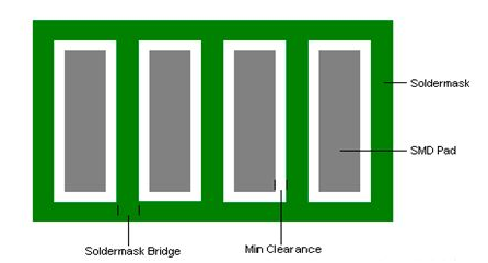
For the bigger picture of how these steps fit into the full build, see our PCB assembly guide and the overview of what SMT is.
NextPCB handles the full range in-house: SMT assembly through automated reflow soldering, through-hole assembly through wave or selective soldering, and mixed-technology boards on the same order. X-ray inspection is applied to BGA and QFN boards to verify joints hidden under the package, and there is no minimum order quantity, so the same process control applies from a single prototype.
Before anything is built, our free DFM/DFA review flags issues that would cause soldering defects, so you can fix them at the design stage rather than after assembly.
Get an Instant Assembly Quote or view our full assembly capabilities.
Neither is better in general. Reflow is better for SMT, and wave is better for high-volume through-hole soldering. Mixed boards often use both.
It depends on the board. Wave lowers the cost per joint on through-hole-heavy boards in volume, while reflow is the most economical route for SMT. For small batches, setup and fixtures can make selective or hand soldering cheaper than wave.
Yes. In mixed-technology assemblies, SMT parts are reflowed first and the through-hole parts are then soldered by wave or selective soldering.
"Flow soldering" is another name for wave soldering used in some regions. It refers to the same process of passing the board over flowing molten solder.
Wave soldering floods the whole bottom side with solder, while selective soldering uses a small programmable nozzle to solder chosen joints only. Selective is better for dense or heat-sensitive mixed boards.
Only small SMD parts glued to the bottom side. BGA, QFN and fine-pitch parts should be reflowed instead.
Use reflow soldering for SMT, wave soldering for high-volume through-hole, and selective soldering when a mixed board has tight keep-outs or heat-sensitive parts. Decide based on component types, board density, volume and inspection needs, and check your layout with a DFM review before production.
Upload your Gerber files for a free DFM check and quote

Still, need help? Contact Us: support@nextpcb.com
Need a PCB or PCBA quote? Quote now