
 NextPCB Capabilities
Printed Circuit Boards
NextPCB Capabilities
Printed Circuit Boards
 PCB Assembly
 Layer Buildup
 SMD-Stencils
 PCB Design-Aid & Layout
 Mechanics
 Quality
 Drills & Throughplating
 Factory & Certificate
 PCB Assembly Factory Show
Certificate
PCB Assembly Factory Show
Certificate
Support Team
Feedback:
support@nextpcb.com


Designing printed circuit boards (PCBs) is a complex and essential process in electronics. Proper PCB routing ensures efficient signal transmission, minimal interference, and optimal performance. This guide comprehensively introduces the ultimate PCB routing guidelines and helps you navigate the various design stages while avoiding common pitfalls.
In this article,

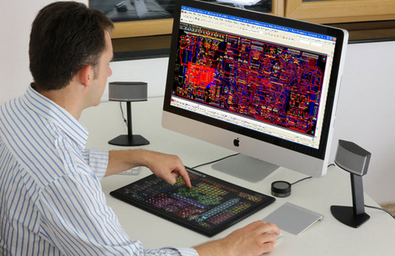
PCB routing is a crucial step in designing PCBs, involving connecting various components on the board to create an efficient and functional electrical circuit. The process builds on component placement, which determines the optimal locations for each component before connecting them with traces or copper lines. PCB routing aims to minimize signal interference, reduce noise, and ensure signal integrity by carefully planning trace paths and adhering to design rules. There are two main approaches to PCB routing: manual and automatic. Manual routing provides more control, while automatic routing saves time and effort using advanced algorithms. Proper PCB routing is essential for high-quality electronic designs.
To achieve optimal performance in your PCB design, following essential PCB routing rules is crucial. These rules help maintain signal integrity, minimize noise, and reduce the likelihood of manufacturing issues. Here are some fundamental PCB routing rules for optimal performance:
Design rules: Follow the manufacturer's design rules and industry standards, including trace width, spacing, and via dimensions. Adhering to these rules ensures your PCB can be fabricated reliably and efficiently.
Prioritize component placement: Optimal component placement significantly impacts the routing efficiency and signal integrity of your PCB. Group related components together, place critical components first, and minimize trace lengths wherever possible.
Route differential pairs correctly: When routing differential pairs, maintain consistent spacing and equal length between the two traces. This ensures proper signal transmission, reduces EMI, and improves noise immunity.
Minimize crosstalk: Increase the spacing between adjacent traces or use ground planes as shields to minimize crosstalk. Consider techniques such as shielding or guard traces for particularly sensitive or high-speed signals.
Match trace lengths: For parallel data transmission or differential signaling, match trace lengths to ensure proper synchronization and signal integrity. Use serpentine patterns or delay lines to equalize the lengths of critical signal traces.
Avoid right-angle turns: Use 45-degree or curved corners when routing traces to maintain a smooth and continuous signal path. Right-angle turns can increase the risk of EMI and signal reflections.
Address thermal considerations: Ensure adequate thermal dissipation by using wider traces for power and high-current paths. Consider heat sinks or thermal vias for high-power components to improve the overall thermal performance of the board.
Conduct design rule check (DRC): After routing, run a DRC to verify compliance with the manufacturer's requirements and industry standards. Fix any violations to prevent fabrication or performance issues.
Ground planes and power distribution play a crucial role in PCB routing, as they significantly impact the circuit's performance, signal integrity, and noise immunity. Let's look at how the ground planes and power can be distributed in PCB:
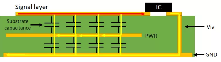
The ground plane is one of the conductive layers in PCB. It works as the common reference point for all the ground connections. It can reduce noise, improve signal integrity and eliminate EMI. Key aspects of ground planes in PCB routing include:
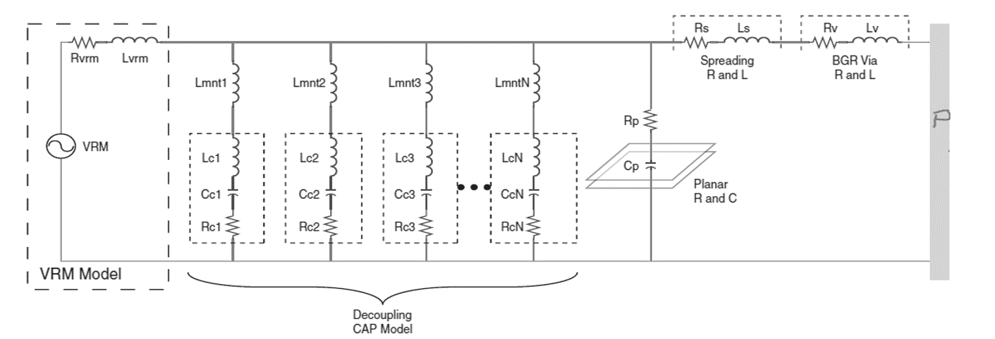
A simplified PDN model
An expertly designed power distribution network (PDN) is essential for preserving stable voltage levels and minimizing noise within a PCB. Important aspects of power distribution in PCB routing include:
You can create a robust and efficient circuit that delivers optimal performance and signal integrity by carefully considering ground planes and power distribution during the PCB routing process.
It is one of the crucial factors to consider while designing PCB. The optimal performance of PCB is determined by eliminating their impact. Below are some of the effective ways to address these challenges in PCB:
PCB routing for RF (radio frequency) and antenna design is essential to optimize the performance of wireless communication. Here are some guidelines to follow when routing PCBs for RF and antenna design:
Use a controlled impedance environment: Maintain a consistent characteristic impedance throughout the RF signal path to avoid reflections and signal degradation. This can be achieved by carefully controlling trace dimensions, dielectric constant, and spacing.
Choose appropriate substrate materials: Use a high-quality, low-loss substrate material with consistent dielectric properties, such as Rogers or FR-4, to minimize signal attenuation and maintain impedance control.
Minimize trace length and bends: Long traces can introduce signal loss and impedance mismatches. Keep RF traces as short and straight as possible. When bends are necessary, use smooth curves instead of right angles to minimize reflections.
Provide adequate grounding: Good grounding is essential for RF performance. Use multiple vias to connect ground planes and provide a low-impedance return path for RF signals. Place vias close to the RF components and along the signal path to reduce ground loop inductance.
Shield critical traces and components: Use shielding techniques, such as guard traces and ground planes, to protect sensitive RF components and traces from external noise and interference.
Consider antenna placement: Place the antenna away from noisy components, such as digital circuits and switching power supplies. Ensure there is sufficient clearance between the antenna and other components or traces to avoid unwanted coupling.
Design matching networks carefully: Impedance matching is crucial for maximum power transfer and minimal reflections. Combine capacitors, inductors, and transmission lines for the ideal impedance match between RF components and the antenna.
Test and Validate Your Designs: Test your design by conducting simulations and measurements to confirm it meets performance requirements, checking signal integrity, impedance matching, and radiation patterns.
Designing a PCB requires attention to detail, and proper routing is crucial for achieving optimal performance, reliability, and manufacturability. Here are some general design tips for PCB routing:
Plan your layout: Before routing, plan your component placement and group related components together. This helps in reducing trace lengths and maintaining signal integrity.
Set up a suitable size for routing traces and placing components. This helps in achieving a more organized layout and makes it easier to modify the design later.
Start with routing power and ground planes, as they often require wider traces and must be distributed throughout the board to ensure proper power delivery and grounding.
Route signals in the same direction as their natural flow, from inputs to outputs. This helps maintain signal integrity and avoid interference between traces.
Shorter traces reduce signal loss, impedance mismatches, and crosstalk. Keep traces as short and direct as possible, especially for high-speed and sensitive signals.
Wider traces have lower resistance and inductance, which benefits power and ground planes. Use a trace width that meets the desired impedance and current-carrying capacity for signal traces.
Sharp angles in traces can lead to signal reflections and electromagnetic radiation. Use smooth curves or 45-degree angles instead.
To minimize crosstalk and interference, keep a sufficient distance between traces. Follow the design rules and guidelines set by the PCB manufacturer for minimum trace spacing.
Vias are necessary for routing signals between different layers but can introduce parasitic capacitance and inductance. Use the minimum number of vias needed and avoid placing vias on high-speed or impedance-controlled traces if possible.
Terminate high-speed and sensitive signals to prevent reflections and ringing. Use series, parallel, or Thevenin termination techniques as appropriate.
Minimize electromagnetic interference (EMI) and ensure electromagnetic compatibility (EMC) by proper shielding, grounding, and trace routing. Keep high-speed signals and clock lines away from sensitive analog components.
Maintain constant spacing and parallel routing for differential pairs to ensure signal integrity and minimize noise and crosstalk.
A ground plane helps in providing a low-impedance return path, shielding sensitive signals, and reducing EMI. Connect the ground plane to component grounds using multiple vias to minimize inductance.
Follow the guidelines and design rules provided by the PCB manufacturer to ensure the design can be fabricated efficiently and cost-effectively.
Perform simulations and measurements to verify that your PCB meets the required performance and reliability specifications. Iterate your design as needed based on the test results.
PCB routing software and tools play a crucial role in designing and organizing circuit boards, ensuring they are efficient, well-organized, and error-free. Some popular PCB routing software and tools include:
Autodesk EAGLE: A user-friendly software popular among hobbyists, students, and professionals, offering schematic capture, board layout, auto-routing, a vast component library, and a supportive user community.
Altium Designer: A high-end, feature-packed software suitable for complex designs, providing powerful schematic capture, PCB layout, routing, 3D visualization, high-speed design features, and extensive libraries.
KiCad EDA: An open-source software favored by hobbyists and professionals, featuring schematic capture, board layout, routing, a large library, ongoing development, and robust community support.
Cadence OrCAD: A comprehensive design suite with schematic capture, PCB layout, routing tools, advanced features like high-speed and RF design capabilities, constraint-driven design, and PSpice integration for circuit simulation.
Mentor Graphics PADS: PADS is a powerful PCB design software with a focus on ease of use and productivity. It offers schematic capture, PCB layout, routing tools, and features like high-speed design, constraint management, and thermal analysis.
CircuitStudio: CircuitStudio is a professional PCB design tool from Altium, focused on ease of use and affordability. It offers schematic capture, PCB layout, routing capabilities, 3D visualization, and an extensive component library.
DipTrace: DipTrace is a user-friendly PCB design software with schematic capture, PCB layout, and routing features. It is suitable for beginners and advanced users alike, offering a shallow learning curve, an extensive component library, and a 3D preview feature.
DesignSpark: PCB is a free, user-friendly PCB design program by RS Components, featuring schematic capture, PCB layout, auto-routing, a vast component library, and 3D visualization.
EasyEDA: It is an online PCB design tool that lets users design and share schematics, PCB layouts, and circuit simulations, providing a comprehensive component library, auto-routing, and integration with JLCPCB fabrication service.
PCB routing is a critical stage in PCB design, building upon the prior component placement step, which determines each component's location. The routing approach you select will hinge on the specific needs of your PCB design.
Still, need help? Contact Us: support@nextpcb.com
Need a PCB or PCBA quote? Quote now


 Surface

