
 NextPCB Capabilities
Printed Circuit Boards
NextPCB Capabilities
Printed Circuit Boards
 PCB Assembly
 Layer Buildup
 SMD-Stencils
 PCB Design-Aid & Layout
 Mechanics
 Quality
 Drills & Throughplating
 Factory & Certificate
 PCB Assembly Factory Show
Certificate
PCB Assembly Factory Show
Certificate
Support Team
Feedback:
support@nextpcb.com


When a circuit is run at a high frequency, its capacitance and inductance are combined to form its impedance. It is somewhat distinct from resistance, which is a DC characteristic, although being measured in Ohms as well. Resistance is unrelated to frequency, whereas this is an AC characteristic.
Impedance control involves monitoring the impedances of certain traces during PCB manufacturing and ensuring that it is within the designer-specified range. Despite being costly, this method gained popularity around the turn of the century due to the increasing electrical components' frequencies. Controlled impedance enables us to ensure that signals are not corrupted as they route through a PCB at high frequencies. Because, where PCB traces do not behave like simple connections. Controlled impedances essentially entails matching substrate material qualities with trace size and locations to guarantee that a trace's signal impedance is within a particular percentage of a given value. High-frequency performance is repeatable with controlled impedance boards.
Controlled impedances should be used when a signal requires a specific impedance to operate appropriately. It's crucial to match the impedance of PCB traces in high-frequency applications to preserve data integrity and signal clarity. There could be longer switching times inside the device or the circuit if the PCB trace connecting two components has a different value from the characteristic impedance of the components. There could also be random errors.
Once the components are installed on the circuit, uncontrolled impedance is hard to analyze. Depending on the batch, components have varying tolerance limits. Additionally, temperature changes have an influence on their requirements and might cause failures. Changing the component can appear as the best course of action. In many situations, however, the problem-causing factor is improper trace impedance.
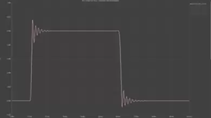
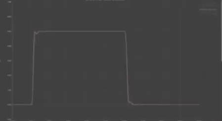
The occurrence of reflections on boards without impedance matching is a significant problem. As a result, some of the signal's energy will be reflected toward the driver, while the remaining signal will go forward. You won't observe a pristine square wave when looking at the waveform for this. Instead, a distorted waveform will be seen, along with occasional ringing, overshoots, and undershoots. On the PCB, any mismatched impedances will cause some electromagnetic interference (EMI). The mismatch in impedances will thus result in some electromagnetic radiation in the specific region where this transition occurs and where these reflections are visible. Plus, the radiation may impact specific vulnerable components on the board or link its energy to nearby traces. Here the below waveforms show how the radiation affects the signal integrity and how the proper termination can be used to reduce that effect.
For this reason, you have to trace impedances and their tolerances early during the of the PCB design process. To ensure the conformance of component values, designers and manufacturers must interact closely.
A PCB trace's conductance, resistance, and inductive and capacitive reactance make up its characteristic impedance. These parameters depend on the physical size of the trace, the PCB substrate material's dielectric constant, and the dielectric thickness. For that, FR-4 PCB material also a material that can be apply.
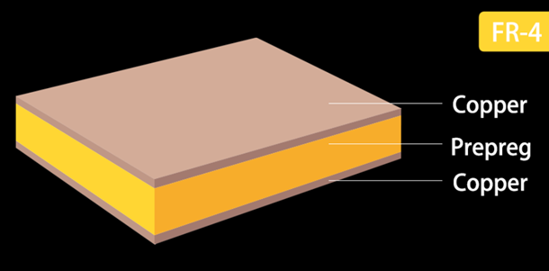
The most popular dielectric substance used in printed circuit boards is FR-4. The term "FR," which stands for "Flame Retardant," denotes that the material achieves the UL94V-0 standard for the flammability of plastic materials. While the grade in the family of glass epoxy laminate materials is indicated by the number 4. When the material burns, this substance guarantees that fire won't spread and will be put out immediately. This base substance divides the copper layers in the PCBs and supports them mechanically. Glass-reinforced epoxy laminate also meets the National Electrical Manufacturers Association (NEMA) specification. For the formation of the substrate, which is a composite material by nature, Fiberglass and epoxy resin will be use as the raw materials
Thus, PCB trace impedance typically falls between 25 and 125 ohms. The following variables will affect the impedance value produced by the PCB structure:
Therefore, the board designer must ensure that their choice of trace and stack up for high-frequency signals enables them to reach the desired impedance value with a specified tolerance. The most sophisticated CAD design programs for electronics automatically compute impedance as follow:
Because their impedances are independent of input voltage, linear elements are the most basic circuit components in a PCB. Basic electronics concepts like Kirchoff's Law and Ohm's Law are applicable to estimating a circuit's impedance, voltage, and current using an AC analysis.
The following formulae represent the overall impedance for a series RLC circuit
R is the DC component, Xl is inductive, and Xc is capacitive.


Since the reactance of both capacitive and inductive components is a function of angular frequency, the total impedance is a complex quantity with real and imaginary parts.

In addition to manual analysis, you may obtain the overall impedance of the circuit and its components by using the Gauss-Jordan approach in SPICE simulators. Transient or pole-zero analysis can assess how the configuration of circuit parts will impact the transition to steady-state behavior in the time domain.
When a circuit incorporates components like diodes, transistors, amplifiers, and other elements whose output is a nonlinear function of input signal intensity, calculating these becomes more difficult. The transimpedance at a specific input signal intensity defines the impedance. In other words, the equivalent impedance of the circuit and the transimpedance of each nonlinear circuit part will vary if the input signal intensity varies.
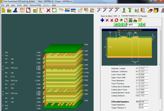
To simplify impedance calculations, NextPCB offers an online PCB Impedance Calculator. With over 15 years of experience in PCB manufacturing, NextPCB's tool enables designers to quickly and accurately determine impedance values, ensuring optimal performance in high-frequency applications.
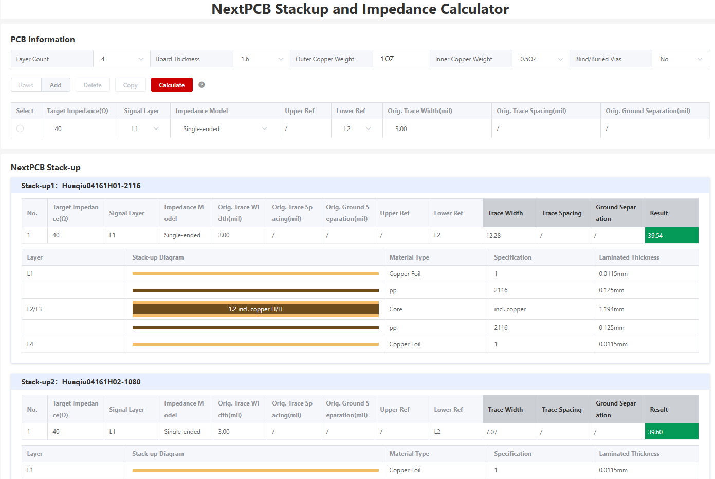
NextPCB Stackup and Impedance Calculator
PCB Impedance Calculator Online
The impedance signals experience on an actual PCB layout may differ much from the ideal value you calculated from a schematic. The main reason for this is substrates's existance and the boad's tracing layout. This results in consequences like crosstalk, which deviates from desirable impedance levels. Power integrity issues like ringing may occur when circuits switch at high frequencies. At higher frequencies, your power delivery network's impedance will also diverge from the optimum capacitive behavior, which might cause issues with signal integrity and power integrity.
The use of high-speed devices is growing; thus, board designers must consider various variables that may affect PCB performance. Impedance control is one of these factors, and it significantly impacts signal integrity and board functionality. The PCB designer may provide a properly designed solution by comprehending the causes of impedance mismatch and learning design techniques to reduce or eliminate impedance difficulties. A strong design may create a dependable and effective printed circuit board.
Still, need help? Contact Us: support@nextpcb.com
Need a PCB or PCBA quote? Quote now


 Surface

