
 Surface


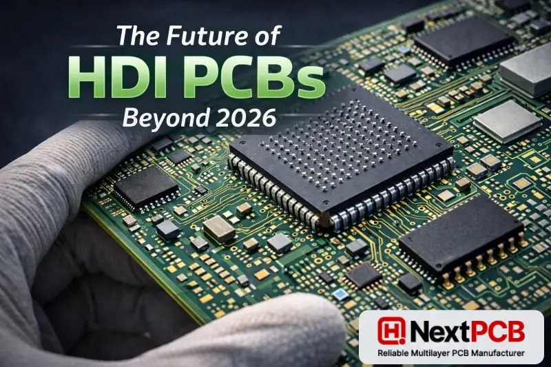
High-density interconnect (HDI) PCB showcasing microvias, fine routing, and advanced BGA packaging, representing the future of compact and high-performance electronics beyond 2026.

 NextPCB Capabilities
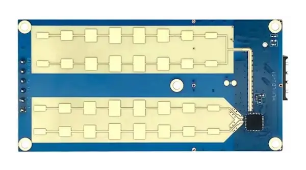
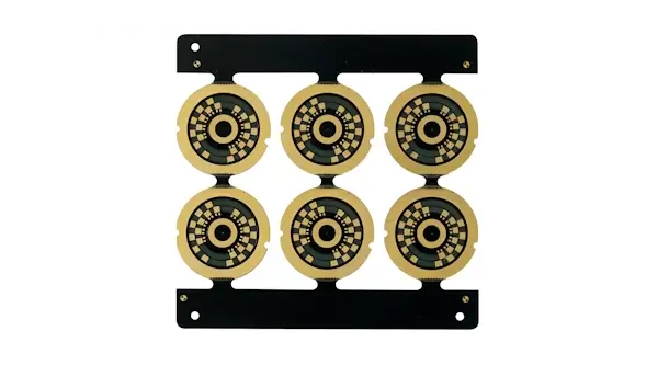
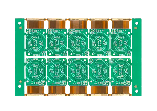
Printed Circuit Boards
NextPCB Capabilities
Printed Circuit Boards
 PCB Assembly
 Layer Buildup
 SMD-Stencils
 PCB Design-Aid & Layout
 Mechanics
 Quality
 Drills & Throughplating
 Factory & Certificate
 PCB Assembly Factory Show
Certificate
PCB Assembly Factory Show
Certificate
Support Team
Feedback:
support@nextpcb.com


Introduction
Printed circuit boards have evolved as electronic devices became smaller and more complex. Traditional multilayer designs reached their limits, leading to HDI PCBs, which use microvias, finer traces, and advanced stackups to deliver higher density and better performance in compact designs.
By 2026, HDI PCBs are essential for applications such as 5G, IoT, ADAS, and medical electronics. They help designers integrate complex components within tight space, power, and thermal constraints. This article explores HDI PCB trends, market demand, sustainability, and key adoption challenges in 2026.
Table of Contents
High-density interconnect (HDI) PCB showcasing microvias, fine routing, and advanced BGA packaging, representing the future of compact and high-performance electronics beyond 2026.
To understand why HDI PCBs are shaping electronics in 2026, it is important to first clarify what HDI technology is, how it differs from conventional PCB designs, and which structural elements make it possible. HDI PCBs are not a single technique but a combination of advanced design and manufacturing approaches developed to overcome the physical and electrical limitations of traditional multilayer boards.
An HDI (High-Density Interconnect) PCB is a printed circuit board that features a significantly higher wiring density per unit area compared to standard multilayer PCBs. This is achieved through the use of microvias, finer traces and spaces, higher layer counts, and advanced lamination techniques. HDI technology enables designers to route more signals, place more components, and achieve higher performance within a smaller board footprint.
Key characteristics of HDI PCBs include:
HDI PCB performance is enabled by several core building blocks that work together to increase density and efficiency:
HDI PCBs are commonly classified by their stackup structures, which describe how HDI layers are arranged around a core.
>> For a systematic overview of common HDI PCB stackup structures—such as 1+N+1 and 2+N+2 classifications—refer to Common HDI Stackup Types (1+N+1, 2+N+2 and More)
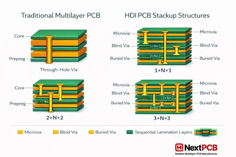
Comparison of traditional multilayer PCB and HDI PCB stackup structures, showing microvias, blind vias, buried vias, and sequential lamination in 1+N+1, 2+N+2, and 3+N+3 designs
This structure consists of one HDI layer on each side of a conventional multilayer core (N). It is often used as an entry-level HDI solution and is suitable for moderately dense designs such as consumer electronics and industrial control boards.
In this configuration, two HDI layers are added to each side of the core. This allows for greater routing density and more complex interconnections. It is commonly used in smartphones, networking equipment, and compact embedded systems.
Advanced HDI designs may use three or more HDI layers on each side of the core. These stackups support extremely high component density, fine-pitch packages, and high-speed signal routing. They are typically found in high-end mobile devices, communication infrastructure, and advanced automotive electronics.
To build these stackups, manufacturers use sequential lamination, where layers are added and bonded in multiple stages. Each lamination cycle allows new microvias and routing layers to be formed. While this increases manufacturing complexity, it provides the flexibility needed to achieve very high interconnect density.
By 2026, HDI PCB technology has advanced well beyond basic miniaturization. Innovations in interconnect structures, materials, and design workflows are enabling higher performance, better reliability, and more predictable manufacturing outcomes. These developments are shaping how engineers approach high-density designs across industries.
Microvia technology continues to evolve as the foundation of HDI PCB design. Improvements in laser drilling accuracy now allow smaller and more consistent microvias, which directly improves yield and reliability.
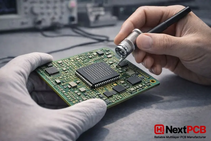
Engineer inspecting an HDI PCB with microvias and via-in-pad under a BGA package, highlighting precision manufacturing and quality control in HDI PCB production
Key developments include:
In practice, these advancements help engineers route complex designs while maintaining manufacturability and long-term reliability.
Miniaturization remains a major driver of HDI innovation. Modern electronics must integrate more functionality into less space without sacrificing performance.
HDI supports miniaturization by enabling:
This is especially important in products such as smartphones, wearables, medical devices, and compact communication modules, where board area directly impacts product size and cost.
As data rates increase, signal integrity becomes a critical design challenge. HDI PCBs help address this by shortening signal paths and improving electrical consistency.
Key performance benefits include:
Combined with low-loss materials, these features make HDI PCBs well suited for high-speed digital and RF applications.
HDI design increasingly relies on advanced tools and tighter integration between design and manufacturing. Modern workflows emphasize early validation to reduce risk.
Current trends include:
The global HDI PCB market is expanding rapidly, with demand projected to climb significantly in the coming years due to miniaturization and connectivity trends. According to industry forecasts, the HDI PCB market was valued at around USD 14.5 billion in 2026 and is expected to grow strongly into the next decade.
Consumer electronics continue to lead HDI demand due to the need for smaller, faster, and more capable devices.
Why it matters: Consumer demand for thinner devices with more features increases reliance on HDI board technology.
HDI is essential in IoT because it enables compact, reliable boards that support connectivity and long-term operation.
Example: Smart meters and environmental sensors use HDI to balance size, connectivity, and energy efficiency.
The rollout of 5G networks has increased demand for boards that handle high-frequency signals.
Market signal: High-frequency PCB demand grew strongly in 2025, driven by 5G and cloud infrastructure.
Automotive and industrial markets require reliable, compact electronics under tough conditions.
Why it’s growing: These sectors increasingly use HDI PCBs to meet performance, safety, and space targets.
Modern HDI PCB manufacturing balances high performance with environmental responsibility. The tables below summarize how sustainability is applied in materials, manufacturing processes, and regulatory compliance—from a practical OEM and engineering perspective.
| Material Choice | Why It’s Used | Practical Benefit |
|---|---|---|
| Halogen-free laminates | Reduce toxic emissions during manufacturing and disposal | Safer production, easier compliance with global standards |
| Low-loss dielectric materials | Minimize signal loss in high-speed designs | Lower power consumption in 5G and networking products |
| High-Tg laminates | Improve thermal and mechanical stability | Longer board life in automotive and industrial environments |
| Moisture-resistant substrates | Reduce delamination risk | Improved reliability in humid or harsh conditions |
| Durable material systems | Extend product lifespan | Fewer repairs and reduced electronic waste |
| Manufacturing Practice | What Changes | Real-World Impact |
|---|---|---|
| Precision laser drilling | Smaller, accurate microvias | Higher yield and less drilling waste |
| Optimized panel utilization | Better board placement per panel | Reduced material scrap |
| Copper recovery systems | Reuse copper from etching | Lower raw material consumption |
| Chemical recycling | Filter and reuse process chemicals | Reduced hazardous waste disposal |
| Closed-loop water systems | Recycle process water | Significant reduction in water usage |
| Energy-efficient equipment | Lower power consumption | Reduced manufacturing carbon footprint |
| Compliance Area | What OEMs Should Know | Why It Matters |
|---|---|---|
| Material restrictions | Limits on hazardous substances | Ensures market access in regulated regions |
| Waste management rules | Controlled disposal and recycling | Reduces environmental and legal risk |
| Emission standards | Stricter manufacturing controls | Encourages cleaner production |
| Global compliance | Multiple regional regulations | Simplifies global product deployment |
| Sustainability reporting | Supplier transparency | Influences OEM supplier selection |
| Green manufacturing practices | Beyond minimum compliance | Builds long-term trust with customers |
HDI PCBs enable compact, high-performance electronics, but adopting them in real projects involves practical trade-offs. In 2026, success with HDI depends less on theory and more on how well design, manufacturing, and supply chain realities are managed.
| Challenges | Practical Solutions |
|---|---|
| Limited availability of specialized materials such as low-loss dielectrics and high-Tg laminates. | Engage suppliers early, finalize material selection during the design phase, and avoid late-stage material changes. |
| High manufacturing complexity due to laser drilling, stacked microvias, and sequential lamination. | Choose the simplest HDI stackup that meets performance needs (e.g., 1+N+1 instead of over-engineering) |
| Tight process tolerances affecting yield and reliability. | Use proven microvia structures, realistic aspect ratios, and validated manufacturing processes. |
| Dependence on skilled labor and advanced equipment. | Work with experienced HDI manufacturers and ensure clear documentation of design intent and fabrication requirements. |
| Higher cost compared to traditional multilayer PCBs. | Evaluate cost at the system level—HDI can reduce board size, connectors, and assembly complexity. |
| Longer lead times due to multiple lamination cycles and inspections. | Perform early DFM reviews and freeze stackup and via structures as early as possible. |
| Risk of delays from late design changes. | Collaborate closely with the manufacturer during layout to validate stackup, routing density, and via strategy. |
| Uncertainty for new adopters or low-volume projects. | Start with HDI prototypes or pilot runs to validate feasibility before scaling production. |
As HDI PCB adoption increases, engineers must carefully decide when HDI is necessary and how to design it efficiently. While HDI offers clear benefits in density, performance, and miniaturization, successful results depend on smart design choices and early coordination with manufacturers.
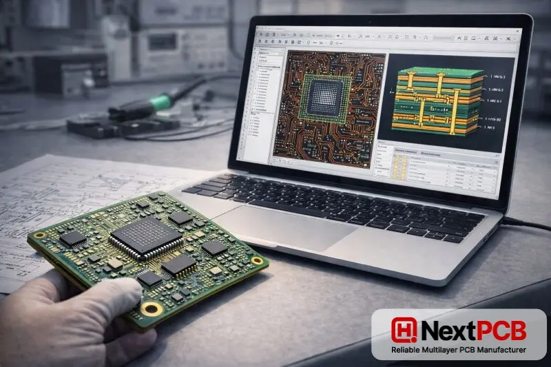
HDI PCB design and manufacturing collaboration, showing a physical HDI board alongside PCB layout and stackup views on design software.
HDI PCBs are best used when traditional multilayer boards cannot meet size, routing, or performance requirements. They are especially suitable for:
Common applications include smartphones, wearables, medical devices, communication modules, and advanced automotive electronics.
Effective HDI design starts with early planning. Selecting the right stackup (such as 1+N+1 or 2+N+2) helps balance cost, performance, and manufacturability. Microvias should be used strategically for signal fan-out, not as a direct replacement for all through-hole vias. Attention to controlled impedance, grounding, and thermal management is essential in dense layouts.
Pushing density beyond manufacturing limits, overusing stacked microvias, or delaying DFM checks can increase cost, reduce yield, and extend lead time. Engineers should always confirm manufacturer capabilities early.
Early collaboration between designers and manufacturers—such as NextPCB—helps validate stackups, materials, and process limits, improving first-pass success and ensuring reliable, high-quality HDI production.
As electronic systems continue to evolve, HDI PCB technology is expected to play an increasingly central role beyond 2026. Ongoing trends in miniaturization, higher data rates, and functional integration are driving demand for PCBs with greater interconnect density, improved reliability, and support for high-speed and high-frequency applications.
HDI development will continue to advance alongside semiconductor and packaging innovations. Smaller components with higher pin counts will require further refinement of microvia structures, finer line and space capabilities, and more advanced stackup designs. At the same time, improvements in low-loss and thermally stable materials will support next-generation communication and RF systems. Greater integration of design automation and simulation tools will also help engineers optimize signal integrity, power delivery, and thermal performance earlier in the design cycle
Beyond consumer electronics, HDI PCBs are seeing growing adoption across automotive, medical, aerospace, industrial automation, and energy sectors. As manufacturing processes mature and global supply chains strengthen, HDI technology is expected to become a standard solution for high-performance electronic systems rather than a specialized choice.
This FAQ section addresses the most common questions to help designers and decision-makers better understand when and how to adopt HDI PCBs.
An HDI PCB is a high-density printed circuit board that uses microvias, finer traces, and advanced stackups to enable compact layouts, improved signal integrity, and high-performance electronics beyond traditional PCB limits.
How does HDI improve signal integrity?
HDI PCBs improve signal integrity by shortening signal paths, reducing via stubs, and enabling controlled impedance routing, optimized grounding, and lower noise, crosstalk, and EMI in high-speed designs.
Are HDI PCBs environmentally sustainable?
Yes, HDI PCBs can be environmentally sustainable through the use of halogen-free materials, improved material efficiency, recycling practices, and compact designs that reduce overall material consumption.
How does HDI affect PCB lead time?
HDI PCBs may have longer lead times due to laser drilling and sequential lamination, but early stackup planning, DFM reviews, and close collaboration with the manufacturer can significantly reduce delays.
Is HDI suitable for low-volume production?
Yes, HDI PCBs are suitable for low-volume production when compact size, high performance, or routing density cannot be achieved with traditional PCBs.
What industries benefit most from HDI PCBs?
Industries that benefit most from HDI PCBs include consumer electronics, IoT, 5G telecommunications, automotive and EVs, medical devices, and industrial automation requiring compact, high-performance electronics.
>> Read More: PCB Lead Time: Why "Advertised" and "Actual" Delivery Dates Are Often Different — And How to Protect Your Schedule
In conclusion, HDI PCB technology is now fundamental to modern electronics and will continue to grow beyond 2026. Advances in microvias, compact design, and high-speed performance are driving adoption across consumer, IoT, 5G, automotive, and industrial applications. At the same time, sustainable manufacturing practices and early design collaboration are essential to managing cost, lead time, and complexity. From a manufacturing perspective, NextPCB supports this evolution by combining advanced HDI capabilities with reliable production processes, helping bridge the gap between innovative PCB design and scalable, real-world manufacturing.
>> Explore More PCB Types
Planning an advanced build? Browse these high-end PCB types and jump to the right capability page.
PCBs made with high glass transition temperature (Tg) materials, typically 170°C and above.
PCBs designed to handle signals in the GHz range with minimal signal loss and distortion.
Circuit boards optimized for high-speed digital signals with careful attention to signal integrity.
High Density Interconnect PCBs with finer lines, smaller vias, and higher connection density.
PCBs manufactured using Rogers Corporation's high-performance laminate materials.
PCBs with exceptionally thick copper layers, typically 3 oz or more, for high-current applications.
Bendable PCBs made with polyimide or polyester substrates for dynamic or space-constrained designs.
Hybrid circuit boards that combine rigid and flexible substrates into a single integrated assembly.
Using ceramic substrates like Al₂O₃ and AlN for extreme thermal and electrical performance.
Still, need help? Contact Us: support@nextpcb.com
Need a PCB or PCBA quote? Quote now

