
 Surface


Julia Wu - Senior Sales Engineer at NextPCB.com

 NextPCB Capabilities
Printed Circuit Boards
NextPCB Capabilities
Printed Circuit Boards
 PCB Assembly
 Layer Buildup
 SMD-Stencils
 PCB Design-Aid & Layout
 Mechanics
 Quality
 Drills & Throughplating
 Factory & Certificate
 PCB Assembly Factory Show
Certificate
PCB Assembly Factory Show
Certificate
Support Team
Feedback:
support@nextpcb.com


Table of Contents
Introduction
As electronic devices become more compact and powerful, thermal management on the PCB is no longer optional—it's foundational. The circuit board itself must function as an efficient heatsink, relying heavily on the superior thermal conductivity of copper to move heat away from critical components. This detailed analysis focuses on the primary mechanism of heat spreading: conduction. We will establish the analytical model necessary to calculate the minimum required copper cross-sectional area under uniform heat load conditions, and critically examine how practical manufacturing limitations, particularly NextPCB's High-Quality DFM (HQDFM) constraints, influence the final copper thickness selection and ensure long-term product reliability.
> Read PCB Thermal Design Series before Practice:
In modern electronic device design, thermal management has transitioned from a mere consideration to a critical engineering constraint. As power density increases and component spacing shrinks, the coupling effects between components become significantly stronger, necessitating that engineers move from traditional component-level analysis to system-level thermal assessment of the circuit board and chassis. This shift demands that design work possess a high degree of predictability and systematic planning.
The reliability of electronic products directly depends on maintaining the component junction temperature (TJ) within specified limits. High junction temperatures lead to multiple negative effects. For instance, high heat can cause increased mechanical stress, accelerated degradation of gate oxides, and increased leakage currents. For transistors, elevated temperatures increase the MOSFET on-resistance (Rds(on)) and reduce the gate-source threshold voltage (Vth), while also slowing down the switching speed of Bipolar Junction Transistors (BJTs).

Designers must proactively control operating temperatures below critical thermal thresholds. The maximum temperature rating (Glass Transition Temperature, Tg) for common FR4 dielectric material is around 130 °C, suitable for standard applications; while high-Tg materials can reach 170 °C or higher, typically recommended for high-temperature or high-density multilayer designs. Any operation exceeding these thresholds will lead to a sharp reduction in product lifespan or catastrophic failure.
Thermal failure often manifests as a positive feedback loop: Component data indicates that rising temperature increases MOSFET on-resistance, leading to higher I²R power dissipation (Joule heating). This increased heat generation further raises the temperature, creating an uncontrolled thermal cycle that eventually causes permanent damage or accelerated performance degradation. Therefore, the goal of active design is to keep the operating temperature well below the 150 °C limit to ensure long-term electrical stability and reliability.
Conduction is the fundamental mechanism for thermal management within the PCB substrate and copper layers. In many cases, the Printed Circuit Board acts as the primary heatsink for attached components. The core goal of the design work is to minimize thermal resistance (Rth). Thermal resistance itself is a function of the heat path length L, material thermal conductivity k, and effective heat transfer cross-sectional area A.
A PCB structure is composed of alternating layers of highly conductive copper and dielectric material (typically FR4/resin). By utilizing copper's high thermal conductivity as an efficient heat spreader, designers transfer heat from the component junction to wider board areas, preparing for subsequent convection and radiation cooling. Although initial design relies on one-dimensional analysis for sizing estimates, the significant coupling effects in modern high-density assemblies mean that these analytical results must ultimately be verified using system-level methods like Computational Fluid Dynamics (CFD) modeling.
Thermal resistance Rth (unit: °C/W) is a measure of how efficiently a structure transfers heat. It equals the temperature difference between two points on a closed surface divided by the total heat flow (Power P):
Rth = (T1 − T2) / P = ΔT / P
Consequently, the temperature rise (ΔT) can be simply calculated as ΔT = P · Rth. In high-power PCB design, the objective is to determine the maximum allowed temperature rise (ΔTallowed), set by the component's maximum allowable junction temperature and ambient temperature, and subsequently calculate the maximum allowable thermal resistance (Rth,allowed) for the structure.
Applicable Scope: Effective when the dominant path is unidirectional conduction and spreading resistance is negligible; spreading resistance or simulation correction should be introduced when significant plane spreading or multiple parallel channels exist.
For preliminary sizing estimates, a one-dimensional steady-state conduction model can be adopted. This model assumes stable, unidirectional heat conduction along the length L of a rectangular slab (or copper bar). In this case, the classical formula for thermal resistance is:
Rth = L / (k · A)
where k is the material's thermal conductivity and A is the cross-sectional area of the heat path. When uniform heat generation exists within a solid and the outer surface is maintained at a constant temperature Ts, the maximum temperature Tmax will occur at the location furthest away from the outer surface.
By substituting the target maximum allowed temperature rise (ΔTallowed) into the thermal resistance formula, the designer can quantify the minimum required cross-sectional area (ACu,min) for the copper conduction path:
ACu,min ≥ (P · L) / (kCu · ΔTallowed)
This formula translates the thermal power budget (P) into a concrete physical geometry requirement (ACu). Since the cross-sectional area ACu equals trace width W multiplied by thickness t (ACu = W · t), and trace width W is often constrained by routing density, increasing copper thickness (t) becomes the primary design means to achieve high-power conduction capacity.
This quantitative constraint forms the basis of the design decision chain: the thermal budget determines the required ACu, which in turn dictates the minimum acceptable thickness (in ounces), and finally, the minimum trace width and spacing are determined by Design for Manufacturability (DFM) rules. This means thermal requirements directly influence the constraints on routing density and board size.
Engineering note: If a conservative effective conductivity keff is used for early estimation, validate the value with CFD and/or measurement during prototyping.
Parallel and bottlenecks: When multiple copper paths or a whole plane conduct in parallel, you may use an effective parallel area Aeq = ΣAi. If there is any geometric neck (fine trace, gap, via neck, split plane), compute by the narrowest section for a conservative and production-realistic result.
The calculation of ACu,min typically assumes the thermal conductivity of pure copper. Where not explicitly stated, all numerical calculations in this article use pure copper kCu = 385–401 W/(m·K) as the baseline; for the equivalent thermal conductivity of the "Copper + FR-4" composite structure, it is explicitly denoted as keff (can be scaled by volume fraction or simulation, engineering conservative value example: keff ≈ 200–300 W/(m·K)). However, the PCB is a composite structure, alternating between highly conductive copper and low-conductive dielectric material (FR4/resin).
For a more accurate evaluation, the effective thermal conductivity (keff) should be used. A widely used method is the weighted volume averaging approach to calculate keff. For modern PCBs, the conductor volume is typically between 10% and 20%. Consequently, the effective thermal conductivity of the inner copper layers is significantly reduced due to the presence of the FR4 dielectric.
Since the manufacturing etching process introduces thickness tolerances (±15% for 2 oz copper and above), this uncertainty must be factored into the model. To ensure reliability, designers should recalculate ACu,min using the worst-case (minimum) copper thickness (i.e., nominal thickness minus 15%). This guarantees that the component's maximum operating temperature limit is met even under unfavorable manufacturing conditions. Therefore, analytical results are considered "preliminary estimates" and must be ultimately verified by CFD simulation tools capable of handling complex boundary conditions and component thermal coupling effects.
The required copper thickness t is specified to the manufacturer in ounces (oz), a unit representing the weight of copper uniformly spread over one square foot of surface area. 1 oz of copper is approximately equal to 0.035 mm (35 µm or 1.37 mil).
For power-intensive PCBs, using 2 oz or even 3 oz copper for power and ground planes is strongly recommended to enhance heatsink function and provide a larger cross-sectional area, thereby reducing voltage drop and minimizing I²R power loss. Heavy copper PCBs are in high demand in high-current applications such as power modules and automotive electronics due to their excellent thermal conductivity, high current-carrying capacity, and mechanical strength.
Terminology: This article collectively refers to ≥ 3–4 oz as Heavy Copper / Thick Copper, and > 20 oz as Extreme Thick Copper.
NextPCB, as a specialized PCB manufacturer, offers 1–2 oz as standard capacity for mass production. For specialized projects, outer layers can be supported up to 4 oz; Extreme Thick Copper (> 20 oz) requires customized assessment. These manufacturing boundaries define the practical limitations for most high-volume designs.
The table below summarizes the conversion of standard copper weights to dimensions:
| Copper Weight (oz) | Thickness (mm) | Thickness (mil) |
|---|---|---|
| 1.0 oz | 0.035 mm | 1.37 mil |
| 2.0 oz | 0.070 mm | 2.74 mil |
| 3.0 oz | 0.107 mm | 4.2 mil |
| 4.0 oz | 0.139 mm | 5.48 mil |
The primary objective of plane design is to maximize the cross-sectional area for conduction heat dissipation. This requires the copper plane to maintain a high degree of uniformity and continuity, avoiding unnecessary segmentation, splits, or voids.
Designers should aim for thermo-electric synergy: an electrically optimized plane (low impedance, continuous return path) inherently constructs the optimal thermal path. Adhering to low-impedance electrical design principles naturally meets the requirements for thermal spreading. Conversely, compromising plane uniformity for supposed signal isolation introduces both electrical impedance and a severe thermal bottleneck.
> Recommend reading: What Factors Affect Characteristic Impedance Precision in High-Speed PCB?
In heavy copper designs, the Coefficient of Thermal Expansion (CTE) mismatch between the thick copper and the FR4 substrate generates significant mechanical stress during thermal cycling (operational phase) and SMT reflow (manufacturing phase).
This stress must be managed through specific design features. Mitigation strategies include: carefully planning stress relief gaps, voids, or slashes alongside large-area heavy copper traces and planes to create expansion relief channels. Furthermore, breaking up long, continuous heavy copper traces into intermittent segments with gaps helps allow for localized expansion and contraction, thereby reducing overall mechanical stress.
Copper balancing is a critical strategy for addressing the thermo-mechanical issues in heavy copper boards. The lack of flatness in heavy copper boards occurs because, during lamination, the areas with a high residual copper rate become thicker than those with a low rate, leading to an uneven surface that is prone to warping during SMT.
The solution is mechanical: ensuring thermal mass symmetry and sufficient resin fill by adding "copper dots" or designing segmented patterns in copper-free areas of inner layers, thus preventing mechanical deformation and ensuring reliable component soldering.

Image adapted from Yuan, Z.; Ding, D.; Zhang, W. Effect of Thermal via Design on Heat Dissipation of High-Lead QFN Packages Mounted on PCB. Applied Sciences 2023, 13(23), 12653. https://doi.org/10.3390/app132312653 (CC BY 4.0). Changes made.
Thermal Vias are essential for vertical thermal management, providing a low thermal impedance path for heat transfer from high-heat component surfaces (typically the thermal pad) to internal ground/power planes or external heatsinks.
The effectiveness of thermal vias depends on the high thermal conductivity of the copper plating inside the via barrel. With copper's thermal conductivity around 385–401 W/(m·K), thermal vias efficiently transfer heat vertically, preventing heat accumulation near components and reducing the risk of localized hotspots and component failure.

Thermal vias must be placed in a dense grid pattern directly beneath the component's thermal pad to minimize thermal resistance from the component junction to the copper plane.
In terms of geometry, typical via diameters range from 0.2 mm to 0.5 mm (8–20 mil). Smaller vias are preferred for high-density designs, while larger vias are used in areas requiring higher heat dissipation capacity. Grid pitch is typically set between 0.8 mm to 1.5 mm (31–60 mil). These dimensions must balance density, manufacturing plating capability, and anti-wicking spacing, and should be based on the component datasheet and the fabrication house's DFM capability.
For Small-to-Mid Power packages like QFN/DFN, typically 5 to 9 thermal vias may suffice; however, large thermal pads or high-power devices require re-optimization of via count/diameter/connected plane thickness based on the target Rth. Regardless of the quantity, vias must be connected to internal ground or power planes through a continuous, solid copper connection to ensure minimal thermal impedance at the layer interface.
> Recommend reading: How to use Standard PCB Stackups for Controlled Impedance
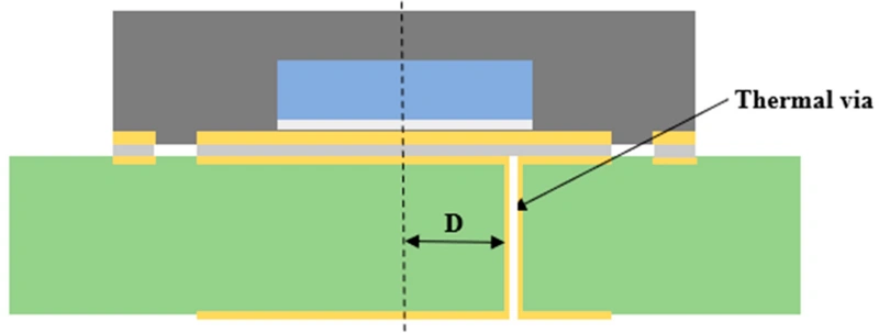
Image adapted from Yuan, Z.; Ding, D.; Zhang, W. Effect of Thermal via Design on Heat Dissipation of High-Lead QFN Packages Mounted on PCB. Applied Sciences 2023, 13(23), 12653. https://doi.org/10.3390/app132312653 (CC BY 4.0). Changes made.
It is crucial to recognize that the effectiveness of thermal vias is limited by the quality of the heatsink they connect to (e.g., internal copper planes). If the internal copper plane is too thin, segmented, or already saturated by heat from other components, no amount of via array optimization will significantly improve performance. This underscores the importance of designing horizontal spreading and vertical transfer as a synergistic thermal system.
During manufacturing, solder wicking is a major challenge. This occurs when capillary action draws solder away from the joint and into the via barrel during reflow soldering, resulting in insufficient solder at the component joint.
Strategies to manage wicking include:
According to the IPC-4761 standard, thermal via treatments can be selected as Type II (Solder Mask Tented) or Type VII (Filled & Capped); for Bottom Terminated Component (BTC) pads, Type VII is often prioritized to balance anti-wicking and pad surface flatness.
In designs with extremely high power density requirements, DFM issues are amplified due to higher internal stresses and tighter manufacturing tolerance requirements. Ensuring DFM compliance is directly related to ensuring thermal reliability and is central to achieving long-term product reliability. NextPCB is committed to providing high-quality PCB fabrication services, making it essential for design engineers to proactively address these challenges at the design stage.
The main challenges in heavy copper design focus on mechanical stability and etching precision.
The following summarizes the Heavy Copper DFM challenges and mitigation strategies:
| DFM Challenge (Heavy Copper) | Thermal/Mechanical Impact | Primary Cause | HQDFM Mitigation Design Strategy |
|---|---|---|---|
| PCB Warpage/Deformation | Open/short circuits due to thermal strain during SMT assembly. | High thermal mass; CTE mismatch between copper and FR4. | Utilize copper dots/segmentation for balancing; implement expansion relief gaps/intermittent traces. |
| Lack of Flatness | Affects SMT assembly quality and final use reliability. | Uneven residual copper rate during lamination leads to inconsistent resin fill. | Maintain high residual copper rate; design symmetry across all layers. |
| Reduced Etching Precision | Trace width reduction post-etching increases Rth and I²R loss. | Higher copper weight requires more aggressive etching, leading to greater undercut and tolerance (±15%). | Significantly increase trace width and spacing; design based on worst-case copper thickness. |
| Via Drill Quality Degradation | Affects vertical thermal performance and long-term connectivity. | Thick copper accelerates drill bit wear. | Optimize inner layer pad design; reduce the number of pads where possible. |
Efficient PCB thermal management is a systemic challenge that requires converting rigorous analytical thermal requirements (Thermal Resistance Rth) into manufacturable physical geometries (Copper Thickness t). By using the one-dimensional steady-state conduction model to calculate the minimum required copper cross-sectional area (ACu,min), engineers can quantitatively determine the necessary copper thickness.
For high-power applications, heavy copper design must be adopted, utilizing its superior horizontal heat spreading capability. This requires implementing continuous, uniform power and ground planes to ensure heat moves rapidly away from the component junction. Concurrently, highly efficient vertical conduction paths must be established using optimized thermal via arrays to transfer heat to inner layers or external heatsinks. Thermal via design must integrate anti-wicking strategies (such as filling or solder mask tenting) to ensure SMT assembly integrity.
Ultimately, the reliability of the design depends on strict DFM validation. For heavy copper PCBs, this is particularly critical, requiring special attention to copper balancing, ensuring trace width and spacing are maintained under manufacturing tolerances, and mitigating thermal cycling-induced mechanical stress through structural symmetry. Only by combining precise conduction analysis with the NextPCB HQDFM principles can a PCB be constructed that operates stably and reliably in high-power density environments.

References
[1] Mauthe, E. A., & Bailey, M. “Modeling the Effect of Thermal Pad Voiding on the Reliability of QFN Components.” SMTA Journal, 2023.
[2] Wang, X., Lin, Y., Xie, Z., et al. “Investigation of Impacts on Printed Circuit Board Laminated Substrate Warpage.” Micromachines, 2021.
Still, need help? Contact Us: support@nextpcb.com
Need a PCB or PCBA quote? Quote now

