
 Surface


Lolly Zheng- Sales Account Manager at NextPCB.com

 NextPCB Capabilities
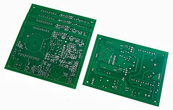
Printed Circuit Boards
NextPCB Capabilities
Printed Circuit Boards
 PCB Assembly
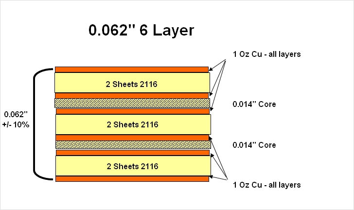
 Layer Buildup
 SMD-Stencils
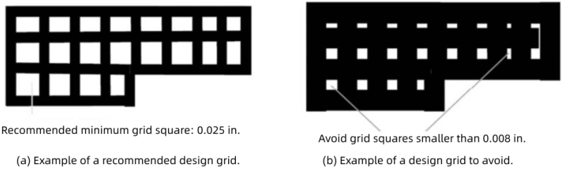
 PCB Design-Aid & Layout
 Mechanics
 Quality
 Drills & Throughplating
 Factory & Certificate
 PCB Assembly Factory Show
Certificate
PCB Assembly Factory Show
Certificate
Support Team
Feedback:
support@nextpcb.com


1. Introduction: The Central Role of Wiring Layout in Thermal Design
Thermal design for Printed Circuit Boards (PCBs) is a systemic engineering task that must be defined and implemented from the architectural level. The first two articles in this series established the foundation: Part 1 focused on substrate material selection, emphasizing the importance of high glass transition temperature (Tg), low coefficient of thermal expansion (CTE), and high thermal conductivity (k) materials; Part 2 focused on component layout, requiring the identification of heat sources, dispersion of high-power devices, and planning of the initial heat flow path.
The Wiring Layout phase is the third, critical step in the thermal design process, translating preliminary thermal management strategies into physical reality. If component layout defines the regions for heat sources and heat sinks, routing is the construction of the high-speed thermal highway connecting these regions. At this stage, designers leverage the excellent thermal conductivity of copper, focusing primarily on managing heat through the conduction mechanism. Conduction capacity is determined by the material's intrinsic thermal conductivity (k), the effective cross-sectional area along the heat path, and decreases with path length. Therefore, the quality of the wiring layout directly dictates how effectively and quickly heat can spread away from the component junction.
Table of Contents
Effective thermal management adheres to fundamental physical laws: the path for heat transfer must be the shortest, and the path's cross-sectional area must be the largest. This principle serves as the core guiding philosophy for PCB thermal design.
At the routing level, this means maximizing the copper area dedicated to the heat conduction path. Maximizing copper area not only reduces thermal resistance (θ) but also simultaneously lowers electrical resistance (R) by increasing the conductor's cross-sectional area. Professional engineers must recognize that any restriction on the heat path (such as thin traces or discontinuous copper planes) will create a thermal bottleneck, leading to a sharp rise in local hotspot temperatures.
Routing design addresses thermal issues from two perspectives: heat source suppression and heat path optimization.
First is heat source suppression. The flow of current through a conductor generates Joule heating (or resistive heating), where power loss (PLOSS) is proportional to the square of the current (I2) and the conductor's resistance (R): PLOSS = R × I2. By using wider or thicker copper traces, resistance (R) can be significantly lowered, directly reducing heat generation and achieving a fundamental improvement in thermal performance.
Second is heat path optimization. The increased mass of copper serves not only to carry current but also as an efficient heat diffuser and conduit. Consequently, adhering to low-impedance electrical design principles (i.e., using wide, thick traces and continuous copper planes) inherently constructs the optimal thermal path. In professional design, electrical integrity and thermal performance are highly synergistic; optimization of one invariably aids the other.
For any PCB trace carrying significant current, its dimensions must be precisely calculated to ensure the temperature does not exceed safety thresholds. The trace temperature (TTrace) is determined by the ambient temperature (TAmbient) plus the temperature rise (ΔT) caused by the current flowing through the trace:
TTrace = TAmbient + ΔT
The design goal is to calculate the required trace dimensions based on the maximum anticipated current, limiting the temperature rise (ΔT) to a safe range.
Controlling trace temperature rise is a critical aspect of reliability engineering. Sustained high temperatures not only degrade component performance but also accelerate material aging and increase the risk of failure. By precisely controlling the amount of Joule heat generated, engineers can ensure the long-term stable operation of electronic products under demanding conditions.
The PCB design industry relies on IPC standards to quantify the relationship between current, temperature rise, and copper cross-sectional area.
IPC-2221 is the foundational standard for determining trace width, providing a simplified, empirical formula that relates current (I), temperature rise (ΔT), and the copper cross-sectional area (A). This formula requires constants k, b, and c derived from curve fitting.
The core formula is:
A[mil^2] = ( I[A] / ( k × (ΔT[°C])^b ) )^(1/c)
Where A is the area in mil2, I is the current in Amperes (A), and ΔT is the temperature rise in °C.
Conversion Tip: 1 oz copper thickness ≈ 35 µm (≈ 1.4 mil); for calculation purposes, copper thickness can also be converted using 1 oz ≈ 1.378 mil.
The position of the trace layer significantly impacts thermal performance. External traces (top or bottom layers) benefit from convection and radiation to the air, thus having a higher k value (k=0.048 for 1 oz copper). In contrast, internal traces dissipate heat primarily through conduction and are less efficient, resulting in a lower k value (k=0.024 for 1 oz copper). The constants b and c are typically set at b=0.44 and c=0.725.
The table below summarizes the key constants used in IPC-2221 for calculating trace cross-sectional area:
| Layer Type | Constant k | Exponent b | Exponent c | Dissipation Characteristic |
|---|---|---|---|---|
| External Layer | 0.048 | 0.44 | 0.725 | Superior, benefits from convection/radiation |
| Internal Layer | 0.024 | 0.44 | 0.725 | Inferior, relies solely on conduction |
Once the trace cross-sectional area is determined, the designer can calculate the required trace width based on the copper thickness.
> Recommend reading: PCB Thermal Design Case Study: Copper Thickness for Uniform Heat Load

IPC-2152 was developed to address the limitations of IPC-2221. Based on more comprehensive experimental data, it considers additional parameters like copper weight, internal vs. external traces, and the external environment, aiming to provide a more accurate temperature rise prediction closer to actual operating conditions.
Since the IPC-2221 formula is based on simplified curves derived from a single board type and copper weight, the IPC admits it may often overestimate the required copper area. IPC-2152 uses a more complex model, and its results will vary based on design conditions (stack-up, copper weight, environment), potentially yielding wider or narrower traces. For high-power, high-reliability designs, engineers should prioritize IPC-2152 guidance, treat the calculated results as the absolute minimum for current safety, and maximize passive heat spreading by incorporating extra thermal margin.
Increasing the thickness of the copper layer is an effective strategy for managing high current and high heat flow. For power-intensive PCBs, 2 oz or even 3 oz copper is recommended for power and ground planes.
Heavy copper PCBs (or thick copper PCBs) offer several significant advantages over standard 1 oz copper:
For applications where current loads are extreme, exceeding the capacity of even thick traces (which typically carry "tens of amperes"), such as high-power industrial or server motherboards, specialized PCB Bus Bars must be considered. PCB bus bars offer ultra-low impedance, superior localized heat dissipation, and can handle several times, or even tens of times, the current of standard wide traces. For designs requiring bus bars, assembly and wave soldering process reviews should be conducted beforehand according to NextPCB's manufacturing specifications.
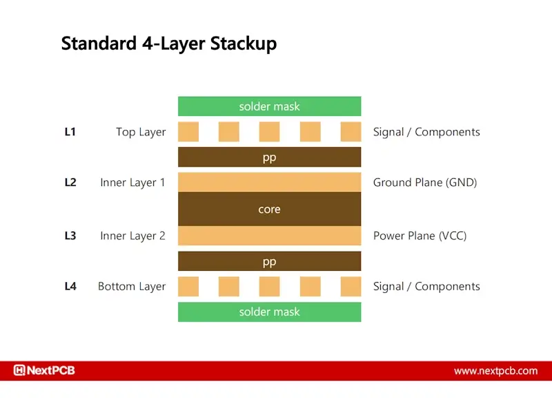
Copper's extremely high thermal conductivity (approx. 400 W/(m·K)) makes it an ideal material for horizontal heat spreading. Designers should leverage multilayer board structures to strategically place large, continuous power and ground planes close to the component layer. This stack-up optimization ensures maximum thermal coupling and heat capture efficiency, helping to rapidly diffuse heat from localized areas into the larger copper body.
In a typical four-layer board, designating the second layer as a solid, uninterrupted ground plane, immediately below the top signal layer, not only creates a microstrip structure for controlled impedance but also establishes the most effective primary heat sink.
For power-intensive PCBs, 2 oz or even 3 oz copper is recommended for power and ground planes. When the heat capacity/current needs to be pushed higher, advanced solutions such as 4 oz (standard) to 6 oz (advanced) outer layer heavy copper, or metal/copper core substrates, are available (covered by NextPCB's capabilities).
> Read How to use Standard PCB Stackups for Controlled Impedance
NextPCB Manufacturing Process and Copper Plane Optimization
Copper planes must maintain uniformity and continuity, avoiding unnecessary splits or voids. This is crucial for achieving low-impedance signal return paths, minimizing Electromagnetic Interference (EMI), and maximizing the cross-sectional area for heat conduction.
From an electrical design perspective, dedicated, continuous ground planes provide low-noise return paths essential for high-frequency Signal Integrity (SI). From a thermal design perspective, a large, uniform copper body offers the best conduction path. Design experience shows that an electrically optimized plane (large, continuous, uniform) perfectly meets the requirements for thermal spreading. Any compromise to plane uniformity (e.g., segmenting for signal isolation) inevitably introduces impedance electrically and creates a bottleneck thermally. Therefore, strictly following guidelines for Signal and Power Integrity, such as establishing solid ground planes, essentially lays the optimal foundation for the thermal management system.
While heavy copper design offers superior electrical and thermal performance, it presents great mechanical challenges. Due to the Coefficient of Thermal Expansion (CTE) mismatch between copper and the FR4 substrate, massive mechanical stress is generated within the heavy copper layers during thermal cycling. If this stress is not managed, it can lead to board warping, delamination, or long-term fatigue failure of solder joints.
For high-reliability designs that must use heavy copper, designers need to perform strategic adjustments to the ideal continuous copper plane, but these methods should be considered options rather than universal rules:
When implementing structural compromises (such as relief gaps or intermittent traces), the designer must validate through thermal simulation or prototyping verification that these adjustments do not cause unacceptable impacts on electrical performance or thermal efficiency.
Thermal vias are small, cylindrical holes drilled into a PCB and filled or plated with conductive material, typically copper. Their primary function is not electrical connection but to conduct heat from the surface heat source (usually the component's thermal pad) down to inner copper layers or external heat sinks.
By minimizing vertical thermal resistance, thermal vias can significantly boost heat dissipation efficiency. Quantitative studies show that well-designed thermal via arrays can effectively reduce component hotspot temperatures by 10°C to 30°C. For example, an AI server GPU motherboard, placing a thermal via array beneath the IC reduced the hotspot temperature from 95°C to 72°C, achieving a 23°C temperature drop, which allowed for system noise reduction.
Optimizing the effectiveness of thermal vias requires precise control over their geometry and placement:
The table below provides key design parameters for optimizing thermal via arrays (Subject to Fab House DFM):
| Parameter | Recommended Range | Design Principle |
|---|---|---|
| Via Diameter | 0.2 mm to 0.5 mm (8–20 mil) | Balance density with manufacturing plating capability. |
| Typical Grid Pitch | 0.8 mm to 1.5 mm (31–60 mil) | Balance thermal spreading with anti-wicking spacing. |
| Placement | Directly under the thermal pad (grid pattern) | Minimize thermal resistance from junction to plane. |
| Connection | Solid copper pour/plane connection | Ensure lowest inter-layer thermal impedance. |
Note: Specific via diameter/pitch should be based on the component datasheet and the fabrication house's DFM capability (e.g., TI QFN recommends ≤ 0.3 mm, 1.0 mm pitch; ADI example uses 0.3 mm, 1.2 mm pitch).
Solder wicking is the primary risk associated with thermal via arrays, especially during reflow soldering of BTCs, where capillary action can draw solder away from the joint and into the via. This can result in voiding, inadequate solder joints, and even potential shorts.
The preferred method for managing wicking is to control the holes using PCB manufacturing processes (IPC-4761 standard):
If thermal vias are intended to transfer heat to the opposite side of the PCB (e.g., the bottom layer) for direct contact with an external heat sink or air, the openings on that side should not be covered by solder mask (i.e., "open window" design). Keeping the window open maximizes heat dissipation through convection and radiation to the environment.
However, it is crucial to note that if thermal vias are located beneath a component's thermal pad and require reflow soldering, to avoid solder wicking, the holes must still be subject to solder mask tenting or plugging during manufacturing, prioritizing manufacturability even when heat export is the ultimate goal.
Thermal Relief Pads (also known as Thermal Ties or Wagon Wheels) are a requirement for Design for Manufacturing (DFM). They connect a through-hole or surface pad to a large copper plane via thin spokes. This is necessary to prevent the large thermal mass of the copper plane from absorbing too much heat during soldering, which would keep the pad temperature below the solder's melting point, resulting in a "cold solder joint."
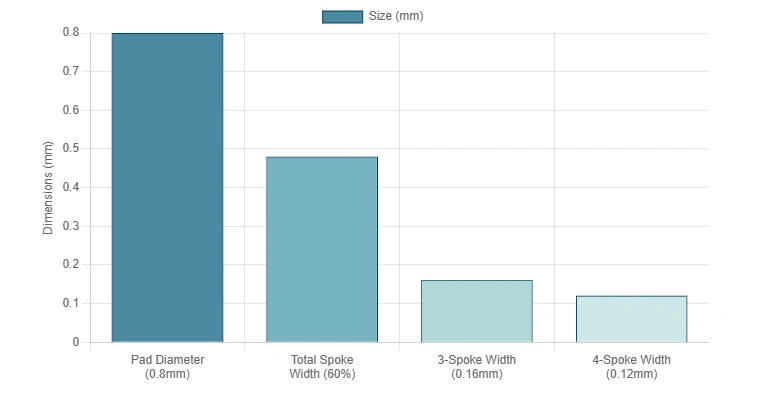
The geometric relationship for thermal relief pads is typically based on industry practice summarized from IPC-2222/MIL-STD-275E. The general guideline is that the Total Thermal Width (cumulative copper area of the spokes) should be limited to approximately 60% of the minimum pad diameter.
The width of each spoke (W) is calculated based on this total thermal width, divided by the required number of spokes (N):
W = (0.60 × DMinLand) / N
Where DMinLand is the minimum pad diameter.
In boards utilizing heavy copper (2 oz or 3 oz), the thermal mass of the large copper planes is significantly increased, necessitating greater thermal isolation (i.e., thinner or fewer spokes) to ensure the solder joint reaches the appropriate temperature. This manufacturing necessity makes the thermal relief pad often the weakest link in the entire thermal conduction path.
To ensure this critical balance point is manufactured precisely, relying on NextPCB's HQDFM (High-Quality Design for Manufacturing) service is essential. HQDFM ensures that in heavy copper, high-density, and complex thermal structures, the critical geometric tolerances (such as spoke width and isolation clearance) are audited to strictly comply with engineering specifications, maximizing design yield and long-term reliability.
| Parameter | Rule/Calculation Basis | Constraint Type |
|---|---|---|
| Total Thermal Width | 60% of minimum pad diameter | Defines DFM/Conduction balance point |
| Spoke Width (N Spokes) | Total Thermal Width / N | Balances heat absorption during soldering |
| Clearance/Opening | Must maintain minimum etch limit | Manufacturing process constraint |
Solder Voiding is a common issue in PCB assembly, usually caused by volatile materials from the flux being released during reflow and trapped by the molten solder.
While research indicates that solder joint voiding may not be the decisive factor in PCB thermal resistance, the presence of voids does reduce the effective contact area of the joint, severely weakening its mechanical resistance to thermal cycling loads and CTE stress. In high-reliability applications, any defect can significantly reduce long-term fatigue life.
Void mitigation often involves optimizing the reflow temperature profile to reduce the release of flux volatiles or using processes like vacuum reflow to facilitate gas escape. By strictly controlling the assembly process, designers can ensure that the solder joint possesses both good electrical conductivity and long-term structural reliability.
Thermal design is a highly iterative and collaborative process. The routing designer must first confirm that component layout (Part 2) has minimized heat accumulation. The sole objective of the routing phase is to provide the most effective conduction connection from the component's thermal pad to the nearest copper heat spreading plane, all while meeting electrical, SI/EMI, and DFM requirements.
Early in the design, professional thermal simulation tools (such as FEA/CFD analysis) must be used to verify that the chosen trace widths, heavy copper thickness, and thermal via arrays provide sufficient temperature margin. It is recommended to start thermal-electrical co-simulation based on IPC-2152 early in the design phase, closing the loop with the fabrication house's capabilities (HQDFM). The design should not be submitted for prototyping without physical or simulated verification.
The final wiring layout must integrate current safety, thermal conduction efficiency, and manufacturing feasibility, transforming the PCB from a passive signal carrier into an active thermal management system. Successful thermal routing design is not just about cooling components; it ensures the entire board structure can reliably withstand the physical stresses of operational temperature extremes, particularly the thermal cycling stress on solder joints and material structures.
Professional PCB designers should follow these key practices:
PCB thermal design is an engineering science that tightly integrates theoretical principles with manufacturing realities. From substrate selection (high Tg, low CTE substrates) to component placement, and finally to routing optimization in this article, every step has a decisive impact on the final product's reliability.
NextPCB, as a professional PCB solution provider, is dedicated to translating cutting-edge engineering theory into highly reliable physical products. Whether you require high Tg, low CTE, or metal/ceramic substrates for high-power applications, or need engineering consultation on heavy copper and complex multilayer stack-ups, NextPCB offers full technical support from instant quotes to HQDFM (High-Quality Design for Manufacturing). By partnering with NextPCB, you can ensure your thermal design solutions are realized with high manufacturing precision, achieving the intended heat dissipation performance and long-term reliability.

References
[1] Ju, C. (2018). The Basic Principles of PCB Wiring Layout for Switching Power. Atlantis Press (ICMCS 2018). atlantis-press.com
[2] Górecki, K., & Posobkiewicz, K. (2023). Influence of a PCB Layout Design on the Efficiency of Heat Dissipation and Mutual Thermal Couplings between Transistors. Electronics, 12(19), 4116. https://doi.org/10.3390/electronics12194116
[3] Huang, Zhiwei. Printed Circuit Board (PCB) Design Technology and Practice (4th ed.). Beijing: Publishing House of Electronics Industry, July 2024. ISBN 978-7-121-31558-9, 672 pp.
Still, need help? Contact Us: support@nextpcb.com
Need a PCB or PCBA quote? Quote now

