

 Printed Circuit Boards
 Surface
 PCB Assembly
 Layer Buildup
 Online Tools
 PCB Design-Aid & Layout
 Mechanics
 SMD-Stencils
 Quality
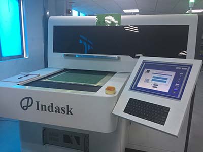
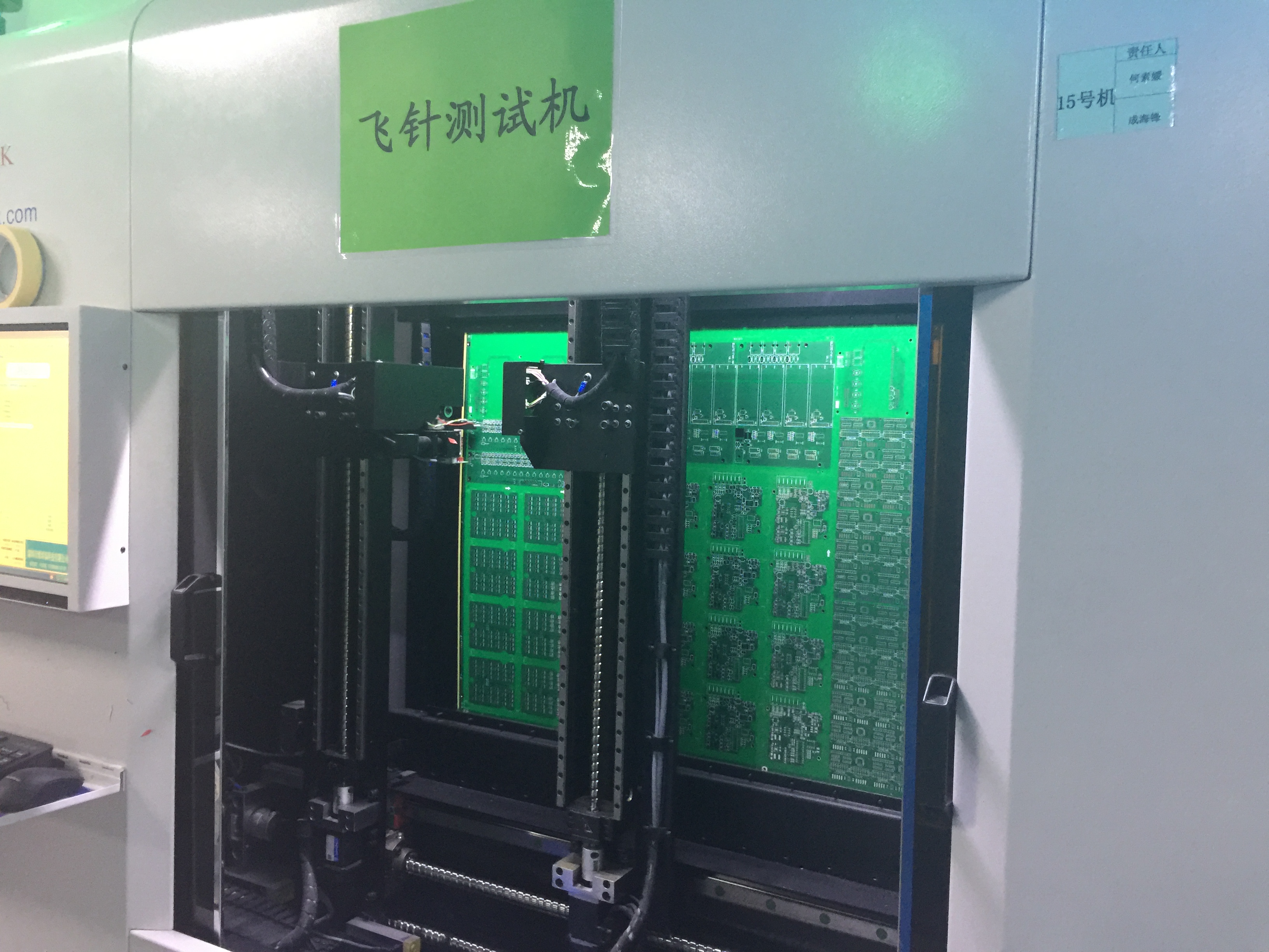
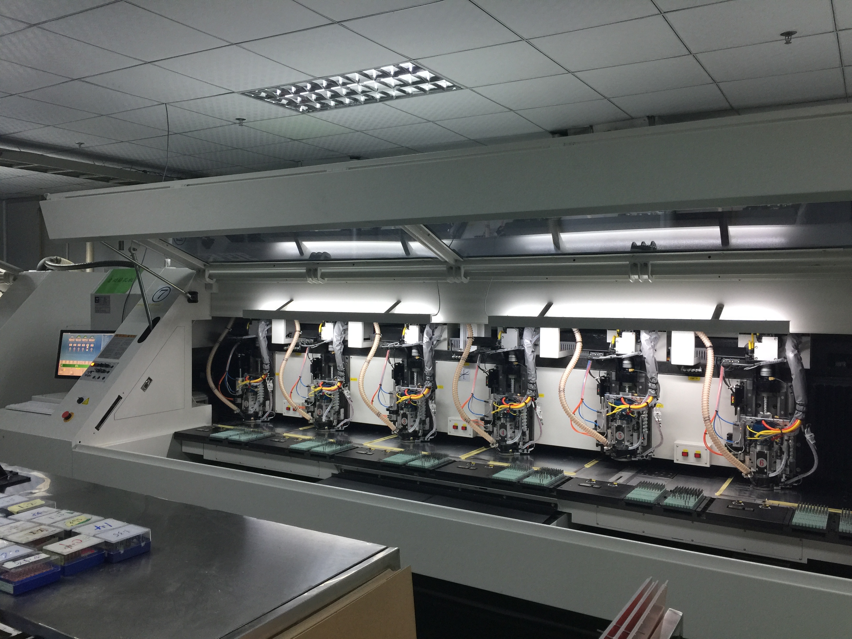
 Drills & Throughplating
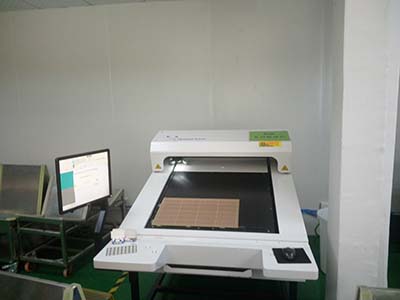
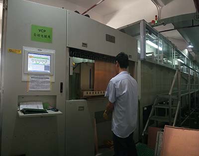
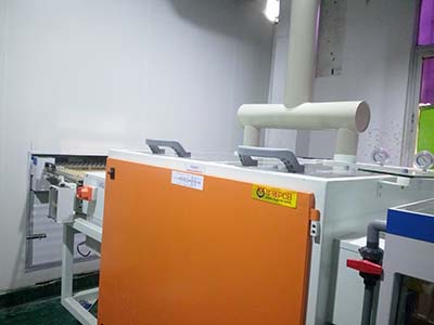
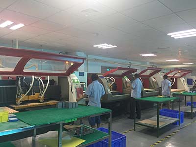
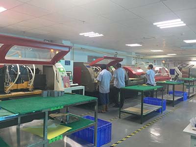
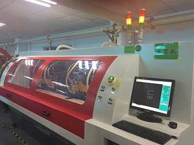
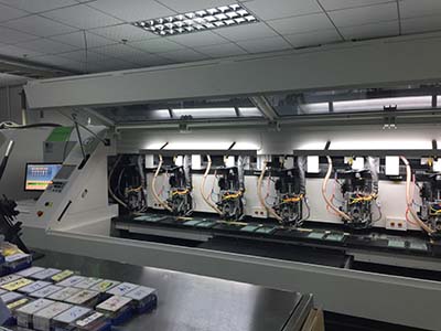
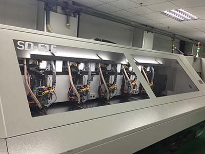
 Factory & Certificate


-
"Smart layout" PCB board
5 Tips
459 1 0 Shares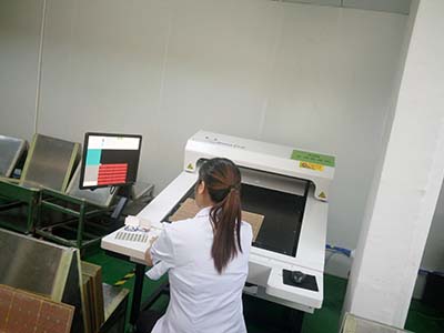
-
-
-
PCB layout technology
In general, the most basic process of designing a board can be divided into three major steps.
3978 1 0 Shares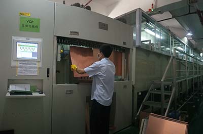
-
-
How to avoid transmission line effects in high speed PCB design?
4 methods and solutions
3867 1 0 Shares
-
-
-
-

-
-
-
-
-
-
-
View layout elements in PCB layout design
1-26 elements
3682 1 0 Shares
-
-
-
What aspects of good PCB design should be considered
Six points
3947 1 0 Shares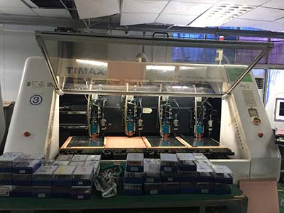
Categories
Recommended Article:
- PCB Stackup for SMT Assembly: Thickness, Copper, Finish — What You Must Specify (and Why)
- PCB & PCBA in Smart Power Grid: Applications, Challenges & Technical Standards
- How to Prepare PCB Files for Assembly: Gerber, BOM, Stackup & More
- 2-Layer or 4-Layer PCB? Don't Let a Few Dollars Difference Ruin Your Circuit Prototype
- Arduino PCB Design Guide for Beginners
- The Ultimate Guide to Choosing Top Printed Circuit Board Manufacturers in 2026
- IoT Application and PCB/HDI Technical Challenges: From Smart Devices to Industrial Gateways
- Arduino Nano Pinout Diagram & Custom PCB Design Guide (2026)
- 4-Layer PCB Stackup Design and Impedance Control
- Cadence Allegro PCB Impedance Control: A Step-by-Step Design Guide