Table of Content
- 1. Raw Material Cost — Is Your Board Material "Over-Luxurious"?
- 2. Panel Utilization Rate — The Profit Hidden in Board Scrap
- 3. Minimum Hole Size and Hole Density — The "Drilling Black Hole" of Time and Material
- 4. Surface Finish Fee (Immersion Gold - ENIG) — The Precious Metal Trap
- 5. Special Processes and Requirements — The Hidden Costs of Non-Standard Processes
- 6. Other Influencing Factors — Procurement and Delivery Surcharges
1. Raw Material Cost — Is Your Board Material "Over-Luxurious"?
Raw materials form the cost foundation of a PCB, but poor selection can easily lead to performance redundancy and financial waste.
1.1 Key Raw Material Factors
1.1.1 The Brand Premium Trap
- Local Brands: Offer high cost-performance ratios, suitable for applications without extreme performance demands.
- Premium Imported Brands: Such as Rogers, Isola, and Panasonic, offer superior performance but come with a significant price premium.
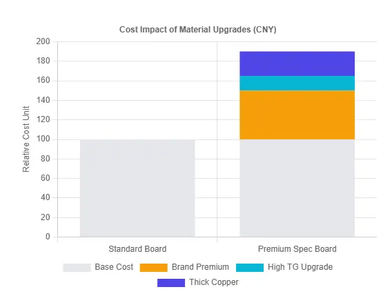
- Same Specification Comparison: For example, Shengyi materials are typically 40-50 CNY per sheet (referring to the single sheet substrate price) higher than Kingboard materials. This difference is substantial in large-volume orders.
1.1.2 TG Value (Glass Transition Temperature) and Heat Resistance
- TG Classification: Standard TG (<150°C), Mid-TG (150-160°C), High-TG (≥170°C).
- Cost vs. Performance: High-TG materials are necessary for lead-free soldering and high-temperature environments, but their unit price is higher. Typically, increasing the TG rating by one level adds 10-15 CNY to the cost. If your product operates in a moderate environment, High-TG is a waste.
1.1.3 Core Thickness
- Thickness vs. Cost: Thicker cores require more base material, resulting in higher material costs.
- Special Thicknesses: Ultra-thin cores (e.g., ≤ 0.1 mm) or extra-thick cores (> 1.5 mm) require custom production and specialized processes, incurring higher prices.
1.1.4 Layer Count and Copper Thickness
- Layer Count: More PCB layers mean an increase in production steps, pressing time, and material usage, leading to a linear increase in cost.
- Copper Thickness: Common specifications include 0.5 oz (≈ 18 µm), 1 oz (≈ 35 µm), and 2 oz (≈ 70 µm). >Learn How Is Copper (Cu) Used in PCB Manufacturing?
- Thick Copper Surcharge: Thick copper increases the difficulty of pressing and etching. A surcharge of approximately 25 CNY/m² per layer is typically added for every 0.5 oz increase in copper thickness.
1.1.5 Other Materials: Solder Mask / Legend Ink
Special color inks (like black solder mask) and imported brand inks cost more than standard green ink.
1.2 Material Selection: Strategies to Maximize Performance and Cost-Efficiency
- Avoid "Over-Engineering" the TG Value: Strictly match the TG value to the product's operating temperature and soldering process (leaded/lead-free). For non-high-heat or non-lead-free environments, selecting Standard or Mid-TG materials can save 10-15 CNY per level.
- Achieve "Cost-Effective Dominance" with Brand Selection: When performance requirements (e.g., Dk/Df) are met, prioritize stable but competitively priced local or mid-range brands.
- Precision Copper Calculation to Prevent Waste: Avoid using unnecessarily thick copper across the entire board. Only design for thick copper in critical areas requiring high current or heat dissipation, thus avoiding the additional 25 CNY/m²/layer processing fee. > PCB Thermal Design Case Study: Copper Thickness for Uniform Heat Load
Standard Copper Weight and Thickness Conversion
| Copper Weight (oz) |
Thickness (mm) |
Thickness (mil) |
| 1.0 oz |
0.035 mm |
1.37 mil |
| 2.0 oz |
0.070 mm |
2.74 mil |
| 3.0 oz |
0.107 mm |
4.2 mil |
| 4.0 oz |
0.139 mm |
5.48 mil |
2. Panel Utilization Rate — The Profit Hidden in Board Scrap
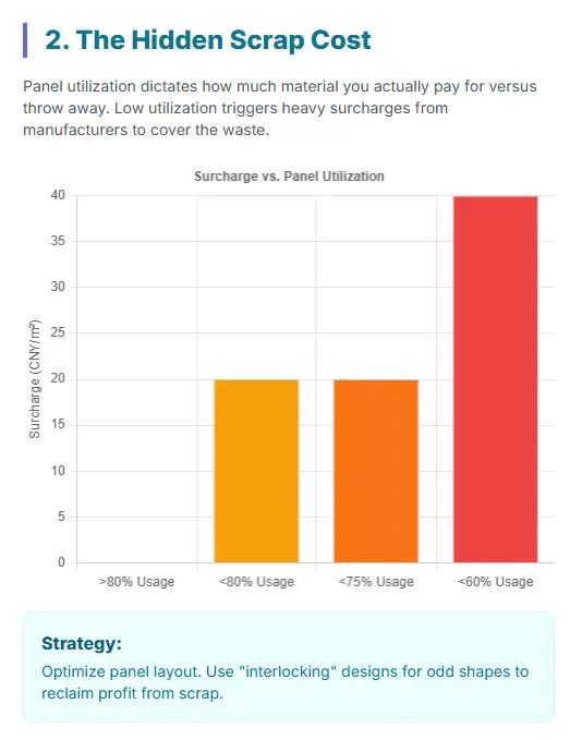
Panel utilization directly dictates the actual material cost you pay for each PCB, making it a blind spot in cost control.
2.1 Key Factors and Rules Affecting Utilization
2.1.1 Critical Points
- Single PCB Size and Shape: Oddly shaped or non-standard size boards are difficult to panelize efficiently.
- Panelization Strategy: Inefficient panelization leads to significant material waste.
> Recommend reading: Complete Guide to Mouse Bite Panelization
2.1.2 Loss Due to Process Constraints
Manufacturers must reserve process edges (e.g., safety margins for SMT component interference, clearance for V-CUT/stamp holes). These areas consume valuable panel space.
2.1.3 Common Surcharges: Penalties for Low Utilization
When utilization falls below industry standards, manufacturers impose surcharges to compensate for material loss:
- Single/Double-Sided Boards: Utilization below 80% incurs a surcharge of approx. 20 CNY/m².
- Multilayer Boards: Utilization below 75% incurs a surcharge of approx. 20 CNY/m².
- Extremely Low Utilization: Boards below 60-70% utilization may incur a surcharge of up to 40 CNY/m².
2.2 Increasing Panel Utilization: Practical Tips for Minimizing Material Waste
Zero Material Waste: Reclaiming Profit through Panel Optimization: Optimize the panel layout. For non-rectangular boards, use "interlocking" or "concave-convex complementary" designs (like jigsaw pieces) to maximize output per large panel.
Standardized Size is King: Aim for single board dimensions that fit the manufacturer's standard panel dimensions and simplify board edges, inter-board spacing, and process auxiliary sizes.
3. Minimum Hole Size and Hole Density — The "Drilling Black Hole" of Time and Material
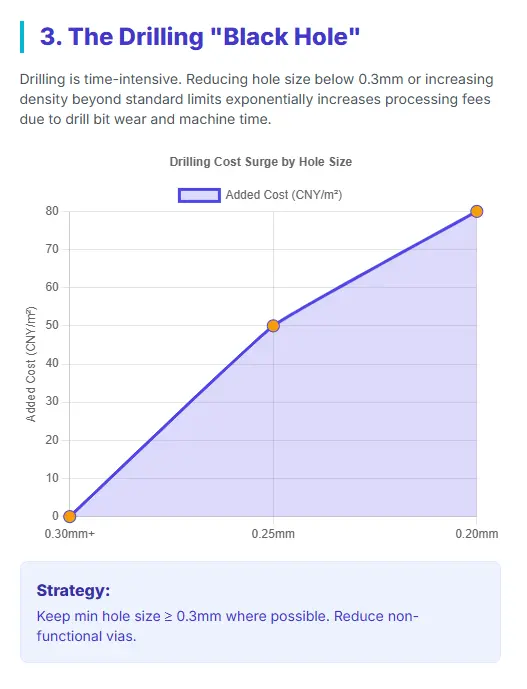
Drilling is one of the most time-consuming and equipment-intensive steps in PCB manufacturing. Small holes and high density directly inflate your processing fees.
3.1 Key Factors Driving Drilling Costs
3.1.1 Hole Size and Processing Difficulty
- Standard Mechanical Drilling Capability: Typically 0.2 mm.
- Difficulty and Cost: Smaller holes increase the risk of drill bit breakage, leading to higher replacement frequency; they also require slower drilling speeds, impacting efficiency.
- Surcharges: < 0.25 mm adds 50 CNY/m²; ≤ 0.2 mm adds 80 CNY/m².
Note: These are approximate figures; specific costs should be confirmed with manufacturers.
3.1.2 Hole Density and Equipment Time
- Cost Drivers: Higher hole counts mean longer running times for the CNC drilling machine, directly increasing: equipment depreciation, energy and labor costs, and production capacity occupation.
- Overage Surcharge: Exceeding industry standards (e.g., ≤ 100,000 holes/m² for 4-layer boards) results in a surcharge of 4 CNY/m² for every additional 10,000 holes.
3.2 Drilling Cost Control: Critical Design Points for Optimizing Hole Size and Density
- Raise Minimum Hole Size to Φ 0.3 mm: Appropriately increase hole sizes to maximize avoidance of the expensive Φ 0.25 mm and below drilling zones.
- Eliminate Non-Functional Vias: Evaluate and reduce the number of unnecessary, non-functional vias in the design.
- "De-densify" Local Areas: For overly dense areas (such as under BGAs), adjust BGA pad pitch to reduce the total number of vias.
> Demystify the complete technical specifics of the PCB Drill File.
4. Surface Finish Fee (Immersion Gold - ENIG) — The Precious Metal Trap
Immersion Gold (ENIG) is a common surface finish, but because it involves precious metals (Nickel + Gold), it is a major source of high cost.
4.1 Key Determinants of Immersion Gold Costs
4.1.1 Global Gold Price Volatility
- Price Fluctuation: ENIG costs are highly sensitive to global gold price changes and require continuous replenishment of expensive chemical Nickel and Gold solutions.
4.1.2 Immersion Gold Area and Thickness
- Immersion Gold Area: A larger area results in higher costs. The area is calculated based on the total surface area of all pads requiring ENIG treatment.
- Immersion Gold Thickness: Thicker plating leads to higher costs.
- Overage Fee: If the ENIG area exceeds a standard percentage (e.g., 20%), an overage fee will be charged proportionally.
4.2 Immersion Gold Cost Control: Rational Selection and Thickness Management from HASL to ENIG
- Rational Alternative Selection: Unless essential functional requirements mandate it (e.g., wire bonding or extremely fine-pitch BGAs), prioritize more economical surface finishes such as Hot Air Solder Leveling (HASL) or Organic Solderability Preservatives (OSP).
- Control Plating Thickness: Specify the minimum acceptable Nickel-Gold layer thickness to meet reliability requirements, avoiding the cost of default over-plating.
- Optimize Solder Mask Openings: Ensure the Solder Mask opening is tightly aligned with the pad edges to minimize unnecessary exposed areas, thereby controlling and reducing the calculated "Immersion Gold Area.
> Recommend reading: HASL vs ENIG: An Ultimate Guide on Surface Finish
5. Special Processes and Requirements — The Hidden Costs of Non-Standard Processes
Any special process that deviates from the standard flow and requires extra equipment or manual labor becomes a cost accelerator.
5.1 Specific Cost Factors of Special Processes
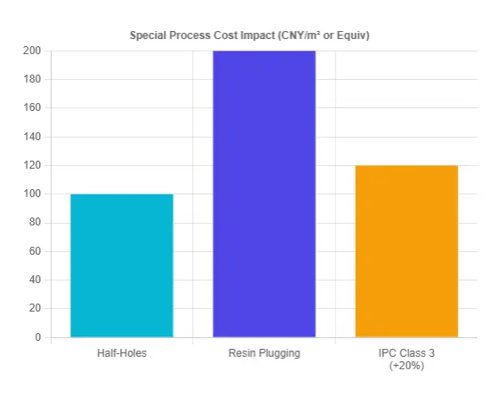
5.1.1 Structural Complexity: Half-Holes and Plugging
Half-Hole/Edge Plating: Minimum surcharge of 100 CNY/m².
Resin Plugging + Plating Fill: Surcharge of approximately 200 CNY/m².
5.1.2 Quality Standard Upgrades
- Standard: Usually shipped according to IPC Class 2 standards.
- IPC Class 3: Requires higher quality, increasing costs by 10-20% depending on layer count and board difficulty.
> Get more information about IPC Class 2 vs 3: The Differences in PCB IPC Standards
5.1.3 Other Special Processes
HDI (High-Density Interconnect), Blue Glue, Carbon Ink, Countersunk Holes, Hard Gold Plating, Press-fit Holes, etc., all lead to increased PCB costs.
>Recommend reading: How HDI Impacts PCB Lead Time?
5.2 Process Complexity Control: Avoiding the Massive Hidden Costs of Non-Standard Flows
- Structural Simplification is Key: Only use half-holes, resin plugging, or similar processes when absolutely necessary for function or structure. For instance, if modular design is not required, avoid half-holes.
- Adhere to IPC Class 2: Where product environment and reliability allow, stick to the standard IPC Class 2 to avoid the 10-20% additional cost of upgrading to Class 3.
- Adopt Standardized Materials: Aim to use standardized materials and structures (like standard green solder mask, avoiding carbon or blue ink) and conventional mechanical processing methods, steering clear of special processes that require custom equipment.
> Other IPC Standards You may interested in: IPC-J-STD-001, IPC-A-610, IPC-A-600, IPC-2581, IPC-2221, IPC-6012
6. Other Influencing Factors — Procurement and Delivery Surcharges
Beyond manufacturing, additional costs in procurement and delivery must be strictly controlled.
6.1 Main Components of Indirect Costs
6.1.1 Testing Costs
Advanced tests like In-Circuit Testing (ICT) are expensive but are cost-effective when distributed across large volumes; they are generally not economical for small batches.
6.1.2 Expedited Turnaround Time (TAT)
Reducing the expected Turnaround Time (TAT) usually means paying a higher expedite fee.
6.1.3 Volume and Packaging
- Quantity: Bulk orders typically secure lower unit costs (economy of scale).
- Packaging: Selecting expensive or overly protective custom packaging materials increases the final cost.
6.2 Procurement and Delivery: Five Key Moves to Minimize Non-Production Surcharges
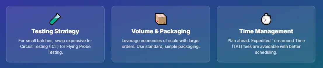
- Optimize Testing Strategy: For small batch or prototype orders, prioritize the use of lower-cost Flying Probe Testing instead of the expensive In-Circuit Testing (ICT).
- Plan Ahead to Avoid Expedite Fees: Plan production and procurement cycles in advance and choose standard delivery times to avoid the expedite fees incurred by shortening the TAT.
- Leverage Economy of Scale: Consolidate order requirements as much as possible to achieve a lower unit price through larger single order volumes.
- Simplify Packaging: Unless the product is extremely sensitive to static or moisture, use standard, cost-effective packaging materials and methods, avoiding complex or expensive custom packaging.
Conclusion
The core of PCB cost is a reflection of manufacturing complexity and efficiency. By integrating DFM (Design For Manufacturing) principles from the initial design phase—rationally assessing material specifications, optimizing drilling parameters, streamlining special processes, and coupling these with effective procurement strategies—you can effectively control your PCB manufacturing costs to a predictable and highly competitive level.
>> Further reading:
> PCB Assembly Cost - Affecting Factors and Way to Save Money
> PCB cost: How Much Does a Printed Circuit Board (PCB) Cost?
> More detailed saving money tips: PCB Cost - 10 Tips to Save Your Money on PCB
About the Author
Lolly Zheng- Sales Account Manager at NextPCB.com
Four years of proven sales experience across electronic components and PCBA industries, with strong expertise in key account acquisition, customer relationship management, and contract negotiations. Focused on driving revenue growth through strategic client development and solution-based selling. Experienced in expanding high-value accounts, securing long-term partnerships, and consistently exceeding sales targets in competitive markets.

 Surface


 NextPCB Capabilities
 PCB Assembly
 Layer Buildup
 SMD-Stencils
 PCB Design-Aid & Layout
 Mechanics
 Quality
 Drills & Throughplating
 Factory & Certificate
 PCB Assembly Factory Show
Certificate
PCB Assembly Factory Show
Certificate


