
 Surface


Lolly Zheng- Sales Account Manager at NextPCB.com

 NextPCB Capabilities
Printed Circuit Boards
NextPCB Capabilities
Printed Circuit Boards
 PCB Assembly
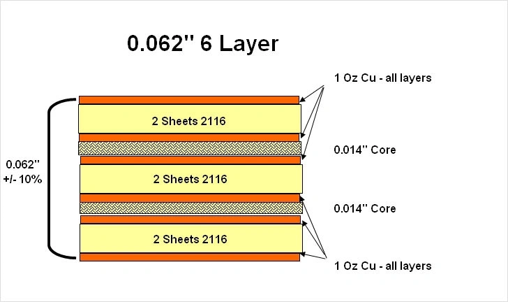
 Layer Buildup
 SMD-Stencils
 PCB Design-Aid & Layout
 Mechanics
 Quality
 Drills & Throughplating
 Factory & Certificate
 PCB Assembly Factory Show
Certificate
PCB Assembly Factory Show
Certificate
Support Team
Feedback:
support@nextpcb.com


Table of Contents
In PCB manufacturing, Cu, copper serves as the primary conductor due to its exceptional electrical and thermal conductivity, malleability, and reliability. Cu, copper is essential for creating traces, determining copper weight, and enabling advanced PCB solutions such as heavy copper, copper coin, and copper-based IMS designs.
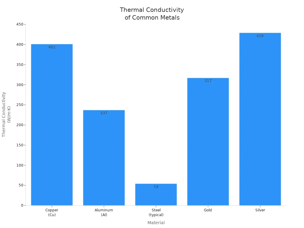
| Material | Thermal Conductivity (W/m·K) |
|---|---|
| Copper (Cu) | 401 |
| Aluminum (Al) | 237 |
| Steel | 16–54 |
| Gold | 317 |
| Silver | 429 |
When you look at a printed circuit board, you see a network of thin lines and large areas made from Cu, copper. These lines are called traces. Traces act as the main highways for electrical signals, connecting different components on the board. The width, thickness, and spacing of these traces play a big role in how well your circuit works. If you design traces with the right size, you help signals move smoothly and reduce the risk of overheating.
You also find copper planes on many PCBs. Power planes deliver energy to all the parts that need it, while ground planes provide a safe path for electrical currents to return. When you use well-designed power and ground planes, you lower electrical noise and improve signal quality. In high-frequency circuits, adding extra copper planes in unused areas creates a low-resistance path for returning current. This helps keep your signals clean and your voltage steady across the board.
The way you arrange copper layers in a multilayer PCB affects how well your board handles signals and power. Good copper layout improves electromagnetic compatibility and reduces interference. NextPCB uses advanced design tools and manufacturing processes to make sure your copper traces and planes meet the highest standards for signal integrity and power distribution.
The term "copper weight" tells you how thick the Cu, copper layer is on your PCB. Manufacturers measure copper weight in ounces per square foot. Here is a simple table to help you understand the common copper weights:
| Copper Weight | Measurement |
|---|---|
| 1oz | 35μm |
| 2oz | 70μm |
| 3oz | 105μm |
If you need a board that can handle more current or heat, you might choose a heavy copper PCB. These boards use thicker copper layers, often 3oz or more. Heavy copper PCBs work well in power electronics, automotive systems, and industrial controls. They help carry large currents and spread heat more effectively, which keeps your devices safe and reliable.
NextPCB offers a wide range of copper weights, including heavy copper options. With precise control over copper thickness, NextPCB helps you design boards that meet your needs for power and thermal management.
Some electronic devices create a lot of heat. For these cases, you can use special techniques like copper coin technology. In this method, you embed a solid piece of Cu, copper inside the PCB. This copper coin acts as a direct path for heat to move away from hot components, such as power amplifiers in base stations. By using copper coins, you protect sensitive parts from overheating and improve the lifespan of your device.
Another advanced solution is the copper-based insulated metal substrate (IMS) PCB. These boards have a metal base, a thermally conductive but electrically insulating layer, and a copper foil on top. IMS PCBs transfer heat much better than standard boards. The special dielectric layer in IMS PCBs is five to ten times more thermally conductive than regular materials. This means your high-power LEDs, automotive modules, or power supplies stay cooler and work more efficiently.
【Tip: Choosing the right Cu, copper application for your PCB can make a big difference in how well your product performs and how long it lasts.】
You measure copper thickness in PCB manufacturing using units like ounces per square foot (oz/ft²) and micrometers (µm). One ounce of copper spread over one square foot equals about 35 microns thick. Manufacturers often use micrometers because this unit gives a precise measurement. For example, 1 oz copper equals 35 microns, while 2 oz copper equals 70 microns. You may also see thickness listed in mils (thousandths of an inch) or millimeters.
Here is a table that shows common copper weights and their thickness:
| Copper Weight (oz/ft²) | Thickness (mils) | Thickness (mm) | Thickness (microns) |
|---|---|---|---|
| 0.5 oz | 0.7 | 0.018 | 18 |
| 1 oz | 1.4 | 0.035 | 35 |
| 2 oz | 2.8 | 0.070 | 70 |
Standard PCBs usually use copper thicknesses from 0.5 oz to 1 oz. High-performance boards may use 2 oz or more. NextPCB offers a wide range of copper thickness options, so you can choose the best fit for your project.
【Note: Selecting the right copper thickness helps you balance performance and cost. Thicker copper layers increase material costs, so you should match the copper weight to your design needs.】
Copper thickness has a direct effect on how well your PCB handles electricity and heat. Thicker copper layers allow more current to flow without overheating. This is important for power electronics, automotive systems, and industrial controls.
When you use thicker copper, you get several benefits:
If you design a board for high-power or high-temperature environments, you should consider using heavy copper, using advanced plating and electroplating processes to ensure uniform copper thickness across large panels. Automated systems help maintain consistent quality, even for complex multilayer boards.
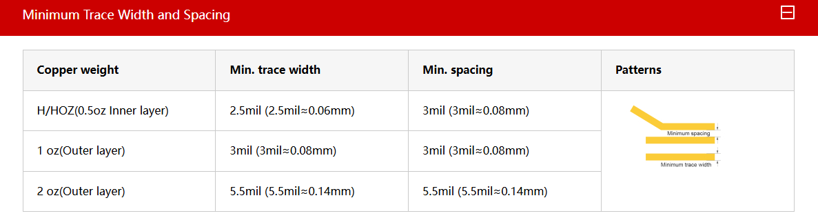
You need to follow industry standards to ensure your PCB meets quality and safety requirements. The IPC (Institute for Printed Circuits) sets guidelines for copper thickness in PCBs. For most applications, the copper thickness ranges from 1 oz to 3 oz. Some special boards may use up to 10 oz or even 20 oz copper for extreme conditions.
| Base Copper Thickness | Maximum Copper Thickness |
|---|---|
| 0.50 oz | 90 microns on track |
| 10 oz |
/ |
| 20 oz | / |
International standards also define copper quality and purity. For example, IS 191:2007 specifies the chemical composition and physical properties of copper used in PCBs. Tests include checking dimensions, chemical makeup, resistivity, and freedom from defects.
【Tip: Always check the copper thickness and quality standards before starting your PCB design. This helps you avoid problems with conductivity, heat, and durability later.】
Cu, copper gives your PCB strong electrical and thermal performance. You boost reliability in harsh environments when you choose the right copper type and thickness. Consider these factors:
Understanding copper applications helps you make better PCB decisions.
What does copper weight mean in PCB manufacturing?
Copper weight tells you the thickness of copper on your PCB. You measure it in ounces per square foot. Thicker copper supports higher current and better heat management.
Why should you choose heavy copper PCBs?
You choose heavy copper PCBs for high-power or high-temperature projects. These boards handle more current and heat. NextPCB offers precise heavy copper solutions for demanding applications.
How does NextPCB ensure copper quality in PCBs?
NextPCB uses advanced plating and strict quality checks. You get consistent copper thickness and high purity. This ensures your PCB meets industry standards for performance and reliability.

Still, need help? Contact Us: support@nextpcb.com
Need a PCB or PCBA quote? Quote now

