
 NextPCB Capabilities
Printed Circuit Boards
NextPCB Capabilities
Printed Circuit Boards
 PCB Assembly
 Layer Buildup
 SMD-Stencils
 PCB Design-Aid & Layout
 Mechanics
 Quality
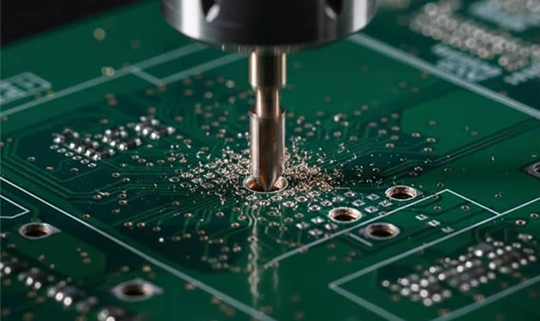
 Drills & Throughplating
 Factory & Certificate
 PCB Assembly Factory Show
Certificate
PCB Assembly Factory Show
Certificate
Support Team
Feedback:
support@nextpcb.com


In the intricate domain of PCB layout/design, engineers frequently dedicate their efforts to optimizing routing/traces, layer stack-up, and component footprint placement. However, there exists one core output file whose accuracy is the direct determinant of successful board fabrication—that is the PCB Drill File (or NC Drill File).
To an entry-level professional in electronics manufacturing, this might merely be perceived as a "hole coordinate listing"; yet, for a seasoned DFM engineer, it represents a critical DFM (Design for Manufacturability) factor that directly governs the project's yield rate and cost structure.
This article will demystify the complete technical specifics of the PCB Drill File.
The drill file, formally termed the NC (Numerical Control) Drill File or colloquially the Excellon Format File, constitutes the CNC instruction set used to command the drilling equipment for precise hole creation. It precisely communicates to the drilling machine: the exact hole location coordinates, the corresponding tool station number (drill bit size), and the operational commands required for the fabrication process. The NC drill file fomat is usually saved with the extensions .drl or .txt.
If you are sending drilling files to the PCB manufacturer, ensure that they include NC Drill format .DRL or .TXT files.
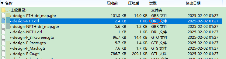
The .drl format for drill file
The .txt format for drill file
In the PCB industry, exporting drill files is a crucial step in PCB fabrication. These files, typically in Excellon or NC Drill format (filename extensions are usually .drl or .txt), tell the manufacturing equipment where and how large the holes should be drilled on the board.
The specific export steps depend on the PCB design software (EDA tool) you are using, such as Altium Designer, KiCad, Eagle. Since the drill file output is usually a part of the overall Gerber generation process, we highly recommend reading our full guide for detailed instructions: > Gerber Files for PCBs: Creating, Viewing, and Converting
| File Type | Description | Manufacturing Function | Format Focus |
| Gerber File | Graphical Data: Shapes and boundaries of traces, pads, silkscreen, and solder mask layers. | Imaging & Etching: Used by the photoplotter to generate films, guiding the copper foil etching process. | RS-274X/X2 (Vector Graphics) |
| Drill File | Positional Data: Precise coordinates and diameters for all holes (PTH, NPTH, vias). | Mechanical Drilling: Used by CNC drilling and laser drilling machines to define exact hole locations. | Excellon (Numerical Control Instructions) |
Summary: The Gerber File defines "where the copper is," while the Drill File defines "where the holes are." Both must share an identical coordinate system to ensure accurate copper-to-hole registration.
A valid NC Drill File must contain the following three critical pieces of information, none can be omitted:
Holes on a PCB are primarily categorized based on their function and inter-layer connectivity, as follows:
| Type | Function | Fabrication Characteristics |
| PTH(Plated Through Hole) | Allows component leads to pass through, and the barrel is copper-plated to connect multiple circuit layers. | Drills through the entire stack-up (Top to Bottom Layer), providing electrical conductivity. |
| NPTH (Non-Plated Through Hole) | Strictly for mechanical purposes (e.g., screw mounting, alignment/tooling pins). The hole barrel is non-conductive. | The barrel is free of copper plating; requires clear segregation from PTH data in the drill file. |
| Through-Hole Via | Connects all layers for signal routing and layer transitioning. | Penetrates all layers of the PCB substrate. |
| Blind/Buried Via |
Blind Vias: Connects an outer layer to one or more inner layers; Buried Vias: Connects two or more inner layers. |
Classified under High-Density Interconnect (HDI) technology, requires separate drill files and sequential fabrication steps. |
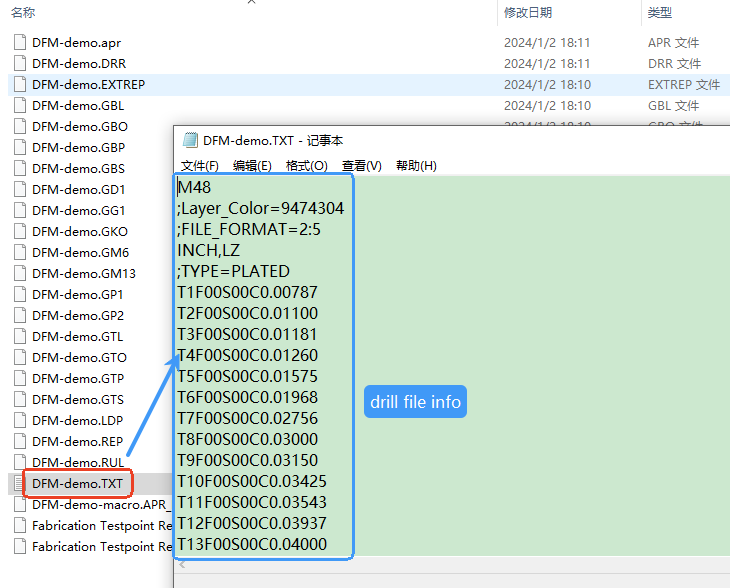
The Excellon Format is a pure text file whose content is a sequence of simple instructions recognizable by a CNC machine tool. Understanding these key commands will help you verify or troubleshoot file errors:
| Command/Parameter | Meaning (Technical Definition) | Example | Notes |
| M48 | Header Start | M48 | The header typically includes critical format definitions and machine parameters. |
| INCH / METRIC | Coordinate Unit Definition | METRIC,TZ | Must be consistent with the coordinate units used in the Gerber files (e.g., inches or millimeters). |
| Txx Cxxx.xxx | Tool Definition | T01C0.800 | Defines the actual finished diameter (0.800mm) corresponding to the specified Tool Number (T01). |
| Txx | Tool Selection | T01 | Instructs the machine to select the tool with the specified index for the subsequent drilling operations. |
| X/Y | Drilling Coordinates | X12500 Y08500 | The precise X/Y location where the drill hit point is required. |
| M30 | Program End | M30 | The mandatory command to terminate the NC program sequence. |
This is the stage where errors are most frequently made and have the most severe consequences when exporting from PCB design software.
A. Coordinate Format and Precision
The format is represented as Integer Digits : Decimal Digits, e.g., 2:4.
B. Zero Suppression
Zero suppression is commonly used to reduce file size and maintain compatibility by omitting zeros in the numbers:
For senior engineers aiming for high-reliability, high-density PCBs, drilling considerations must be integrated into the DFM (Design for Manufacturability) process.
| DFM Rule | Definition/Meaning | DFM Risk Factor | Recommended Value (IPC Class 2) |
| Minimum Hole Size (Diameter) | The smallest diameter that a mechanical drill bit can produce. | Diameters that are too small may necessitate more expensive laser drilling (microvias). | Mechanical drilling generally ≥0.3mm. |
| Aspect Ratio (AR) | The ratio of board thickness to hole diameter (Board Thickness/ Hole Diameter). | An excessively high AR can lead to uneven copper plating on the hole wall, compromising conductive reliability. |
Typically recommended ≤ 10:1 |
| Annular Ring (AR) | The width of the copper ring between the edge of the pad and the finished hole diameter. | Insufficient AR (or drilling misregistration) can cause breakout (drilling off the pad) or pad severance. | Recommended ≥0.15mm |
| Drill-to-Copper Clearance | The distance from the edge of the hole to the nearest copper feature (trace/plane). | Insufficient clearance can lead to shorts or issues with manufacturing tolerances. | Recommended ≥0.2mm(8mil) |
Check Your Designs with Our Free DFM Tool
In High-Density Interconnect (HDI) or complex multilayer boards, non-through-hole structures are necessary to conserve routing space:
Since these vias require sequential drilling and staged lamination (step-by-step pressing), you cannot include their data with standard through-holes.
Non-Plated Through Hole (NPTH) data must be rigorously separated from Plated Through Hole (PTH) data.
To ensure your design transitions smoothly into production, perform a final check against the following list before submitting files to the manufacturer:
Maximizing the quality of this often-underestimated 'blueprint' is the key to guaranteeing your project's timely and high-yield delivery!
All Files Ready? Get Your Price Online
Still, need help? Contact Us: support@nextpcb.com
Need a PCB or PCBA quote? Quote now


 Surface

