

 NextPCB Capabilities
 PCB Assembly
 Layer Buildup
 SMD-Stencils
 PCB Design-Aid & Layout
 Mechanics
 Surface
 Quality
 Drills & Throughplating
 Factory & Certificate


Zhang
Introduction
This article provides a technical deep dive into electronic components, segmented into three critical categories: Passive, Active, and Electromechanical/Optoelectronic. For PCB designers and hardware engineers, this guide moves beyond basic identification to focus on the quantifiable parameters that directly influence system performance—namely Signal Integrity (SI), Power Integrity (PI), and Thermal Management. The component landscape is undergoing rapid transformation, driven by the shift towards high-speed computing, automotive electronics, and the adoption of third-generation wide-bandgap materials like Gallium Nitride (GaN) and Silicon Carbide (SiC). Understanding the non-ideal characteristics of these components (such as parasitic effects) and the thermal demands of advanced ICs is paramount to achieving reliable, high-density system design. This article serves as a practical reference for component selection and design strategy in modern electronics.
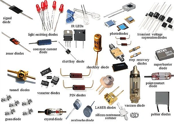
Table of Contents
- - 1.1 Engineering Classification of Electronic Components and System Performance Constraints
- - 1.2 Performance Limits and the Materials Revolution: The Strategic Value of GaN/SiC
- II. Specific Analysis: Types, Parameters, and Practical Considerations of Core Electronic Components
- 2.1.1 Capacitors: Stores of Electrical Charge
- 2.1.2 Resistors: Opposers of Current Flow
- 2.1.3 Inductors: Tools for Storing Magnetic Energy
- 2.3.1 Connectors
- 2.3.2 Sensors
- 2.3.3 Optoelectronic and Display Components
- III. Conclusion: Future Challenges and Skill Requirements for Engineers
- 3.1 Core Design Skill Upgrade: From Component to System
- 3.2 Conclusion and NextPCB Promotion: Transforming High-Performance Design into Reliable Products
I. General Discussion: Component Classification and the Engineering Definition of Performance Boundaries
1.1 Engineering Classification of Electronic Components and System Performance Constraints
In modern hardware design, the electrical characteristics, physical dimensions, and packaging structures of components are the physical cornerstones for achieving product functions, meeting performance indicators (such as high speed and high efficiency), and ensuring product reliability (such as thermal management and shock resistance). Electronic components can be refined into three major engineering categories based on their function in a circuit:
| Classification | Definition | Core Impact on PCB Design | Key Engineering Focus |
|---|---|---|---|
| Passive Components | Definition: Passive components are the "infrastructure" of electronic circuits. They lack the ability to amplify, switch, or process signals, but they are crucial for stabilizing and shaping signals. They operate by storing electrical energy (capacitors), storing magnetic energy (inductors), or consuming electrical energy (resistors). | Parasitic effects (ESR/ESL), impedance matching, loop area. | Tolerance, rated power, Q factor, Isat. |
| Active Components | Definition: Active components are the "brain" and "executors" of electronic circuits. They require continuous external power to function and possess the ability to alter signal characteristics, such as amplifying weak signals, executing high-speed switching (controlling current flow) or executing complex logic operations. | Power Delivery Network (PDN), high-speed routing, thermal design. | RθJC, switching speed (fT), energy efficiency, pin density. |
| Electromechanical/Optoelectronic Components | Definition: Electromechanical/Optoelectronic components are the bridge connecting the "electronic world" and the "physical world." They are responsible for physical quantity/electrical signal conversion, physical connection, or human-machine interaction, serving as the system's input/output (I/O) interface. | Mechanical reliability, EMC/shielding, interface standards. | Rated voltage/current, insertion cycle life, optical parameters. |
1.2 Performance Limits and the Materials Revolution: The Strategic Value of GaN/SiC
The history of electronic component evolution proves that any design is constrained by the physical boundaries of materials and structure (such as ENIAC's 160 kW power consumption). The core challenge in modern design lies in breaking through the "thermal wall" and switching speed limitations of silicon-based materials. Third-generation semiconductor materials (GaN/SiC) hold strategic value because they offer superior high bandgap and high breakdown electric field characteristics compared to traditional silicon devices, making them essential for realizing next-generation high-power-density and high-efficiency systems.
> Recommend reading: What is P-type Semiconductor and N-type Semiconductor?
II. Specific Analysis: Types, Parameters, and Practical Considerations of Core Electronic Components
2.1 Passive Components: Parasitic Challenges in High-Frequency Circuits and Selection Guide
2.1.1 Capacitors: Stores of Electrical Charge
Definition and Description: A capacitor is a component that stores electrical energy (charge), with its energy stored in the form of an electrostatic field. It consists of two adjacent conductors (electrodes) and an insulating dielectric. The primary functions of a capacitor in a circuit include energy storage (as power backup), DC blocking while allowing AC signals through, decoupling (absorbing transient currents to stabilize voltage), and filtering (smoothing power ripple or selecting specific signal frequencies).
| Specific Type | Definition/Description | PCB Engineer Key Parameters | Design Considerations |
|---|---|---|---|
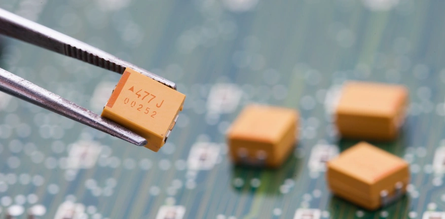
| Multilayer Ceramic Capacitor (MLCC) | Definition: A capacitor constructed by stacking multiple layers of electrodes interleaved with ceramic dielectric layers. | ESR: determines loss and heat; ESL: determines high-frequency decoupling capability; Temperature Coefficient of Capacitance (TCR). | Use small packages (0201/0402) to minimize ESL; be aware of capacitance drop due to DC bias. |
| Tantalum Capacitor | Definition: A capacitor using Tantalum as the anode material and Tantalum Pentoxide as the dielectric. | Rated Voltage (Rated V): sufficient derating margin is necessary; ESR. | Small size, large capacitance, but sensitive to surges and reverse bias, requiring strict derating. |
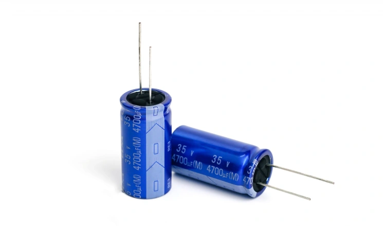
| Aluminum Electrolytic Capacitor | Definition: A capacitor using electrolyte as the cathode, typically offering very large capacitance values. | Capacitance, Ripple Current (Iripple): determines lifespan and heating; Life Cycle. | Lifespan is highly affected by temperature; mainly used for large capacity energy storage and low-frequency filtering. |
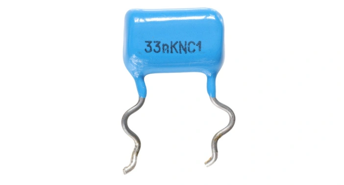
| Film Capacitor | Definition: A capacitor using plastic film as the dielectric. | Pulse endurance, Insulation Resistance. | Offers high stability and low loss, commonly found in high-power, high-voltage applications like electric vehicle chargers (OBC/inverters). |
2.1.2 Resistors: Opposers of Current Flow
Definition and Description: A resistor is a component that consumes electrical energy by impeding the flow of current, serving purposes such as current limiting, voltage/current division, and impedance matching. Its core parameter is the resistance value (Ohms). Resistors convert electrical energy into heat, representing the main form of energy dissipation in a circuit. In precision circuits or high-speed data transmission, the resistor's tolerance and thermal stability are critical.
| Specific Type | Definition/Description | PCB Engineer Key Parameters | Design Considerations |
|---|---|---|---|
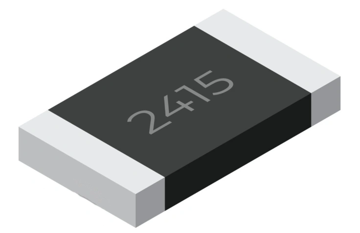
| Chip Resistor | Definition: Common surface-mount technology (SMT) thick-film or thin-film chip resistors. | Resistance Tolerance; Power; TCR (Temperature Coefficient of Resistance): affects precision circuit accuracy. | Select low-TCR resistors to ensure accuracy in precision analog circuits. |
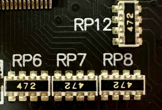
| Resistor Array | Definition: Multiple resistors integrated into a single package. | Channel-to-channel matching, package size. | Used for bus termination and pull-up/pull-down functions, simplifying routing and reducing component count. |
| Thermistor | Definition: A component whose resistance value changes significantly with temperature. | B-value (resistance-temperature characteristic coefficient), R25 value (resistance at 25°C). | Used for temperature sensing or suppressing inrush current during power-up (NTC type). |
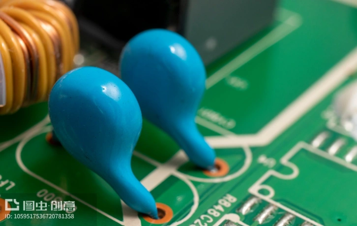
| Varistor | Definition: A component whose resistance changes non-linearly with voltage, primarily used for surge protection. | Clamping Voltage (VCL): voltage level maintained after absorbing a surge; Maximum Surge Current. | Placed at the input port, serving as a transient voltage suppression component. |
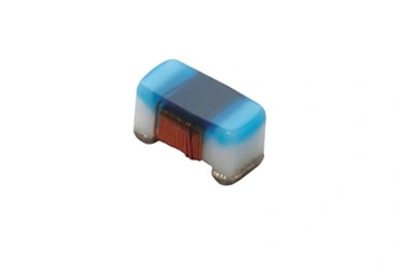
2.1.3 Inductors: Tools for Storing Magnetic Energy
Definition and Description: An inductor is a component that stores electrical energy, with its energy stored in the form of a magnetic field. It is typically constructed by winding a conductor and functions in circuits for energy storage (a key component in switching power supplies), filtering (high-frequency choking, current smoothing), and impedance matching. Inductors maintain current stability through their opposition to current change (self-inductance).
> Recommend reading: Common inductors, transformer detection methods and experience
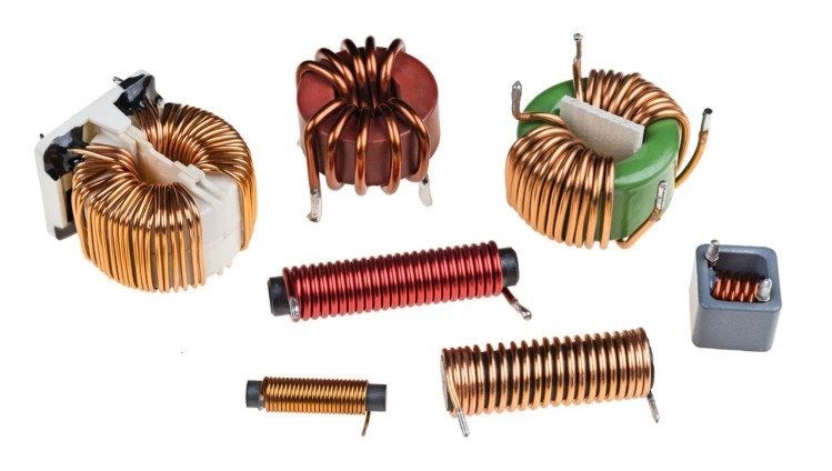
| Specific Type | Definition/Description | PCB Engineer Key Parameters | Design Considerations |
|---|---|---|---|
| Power Inductor | Definition: Used for energy storage and filtering in switching power supplies (SMPS), typically featuring a magnetic core. | Saturation Current (Isat Ferrell): current level at which inductance rapidly decreases; DCR (DC Resistance). | Isat is a critical safety parameter, must strictly control operating current; DCR affects efficiency and heat. |
| RF Inductor | Definition: Used for high-frequency resonance, filtering, and matching, typically air-core or small chip types. | Q Factor (Quality Factor): higher Q means lower loss; Self-Resonant Frequency (SRF). | Must ensure operating frequency is well below the SRF to maintain inductive behavior. |
| Transformer | Definition: A device that uses the principle of electromagnetic induction to transform AC voltage, current, and impedance ratios. | Coupling coefficient, turn ratio, insulation rating. | Common in isolated switching power supplies and network communication interfaces (isolation). |
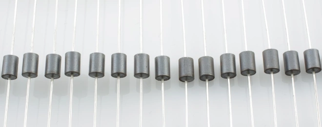
| Ferrite Bead | Definition: Made of ferrite material, exhibiting high impedance at high frequencies, used to suppress EMI noise. | Impedance Frequency Curve (typically impedance at 100MHz). | Avoid placing too many in series in the power path, as this can cause power rail oscillation. |
2.2 Active Components: Performance, Power Consumption, and New Material Integration
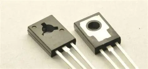
2.2.1 Semiconductor Discrete Devices
Definition and Description: Discrete devices are the most fundamental semiconductor components of modern electronic circuits, including diodes and transistors. They are called "discrete" because each component is individually packaged and performs a single, distinct function (e.g., only allowing unidirectional current flow, or only controlling switching). Discrete devices offer high design flexibility and customization, often providing advantages over integrated circuits in specific applications that require handling large currents, high voltages, or high frequencies. Discrete devices are the physical foundation of power conversion, signal conditioning, and protection circuits.
> Recommend reading: Chips and Wafers: Making of the semiconductor industry
> Recommend reading: What is P-type Semiconductor and N-type Semiconductor?
| Specific Type | Definition/Description | PCB Engineer Key Parameters | Design Considerations |
|---|---|---|---|
| Diode | A two-terminal semiconductor component functioning like a one-way valve, allowing current to flow in only one direction. Primarily used for rectification and circuit protection. | Forward Voltage Drop (Vf); Reverse Recovery Time (trr): determines loss in high-frequency applications. | Schottky diodes have low Vf and extremely short trr, suitable for high-frequency rectification and clamping. |
|
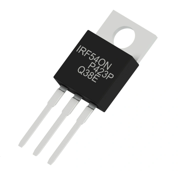
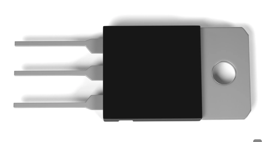
Conventional Power MOSFET |
The most commonly used "electronic switch," controlling the opening or closing of a large current path via a gate voltage. Primarily used for power switching and signal amplification. >IRFZ44N | On-Resistance (RDS(on)); Gate Charge (Qg); Junction-to-Case Thermal Resistance (RθJC). | Lower RDS(on) means lower loss; smaller Qg simplifies gate driving. |
| Silicon Carbide FET (SiC FET) | A transistor manufactured using the third-generation semiconductor material, Silicon Carbide. Compared to silicon, it operates stably at higher voltages and temperatures (high breakdown voltage), suitable for high-voltage and high-power applications. | Voltage rating; RDS(on); Body diode performance. | Suitable for electric vehicle inverters and high-voltage industrial power supplies. |
| Gallium Nitride FET (GaN FET) | A transistor manufactured using the third-generation semiconductor material, Gallium Nitride. Noted for its extremely fast switching speed, enabling higher efficiency and power density, making it crucial for high-frequency power modules. | Switching speed (dv/dt and di/dt); RDS(on); Low RθJC. | Ultra-high frequency, high-efficiency switching, requiring parasitic inductance of the power loop to be minimized to control EMI. |
2.2.2 Integrated Circuits (IC)
Definition and Description: The Integrated Circuit (IC) is the core of modern electronic systems. It integrates tens of thousands or even billions of tiny transistors, resistors, capacitors, and the metal interconnects that link them, all fabricated and packaged onto a minuscule silicon wafer (Chip) using precision semiconductor manufacturing processes. The core value of an IC lies in its extremely high integration density, complex functionality, and tiny size, enabling it to perform a vast range of functions, from complex Central Processing Units (CPUs) to simple operational amplifiers. For PCB designers, the IC's packaging, power consumption, and high-speed I/O interfaces define the maximum difficulty in routing and thermal dissipation, serving as the integrated manifestation of system performance.
| Specific Type | Definition/Description | PCB Engineer Key Parameters | Design Considerations |
|---|---|---|---|
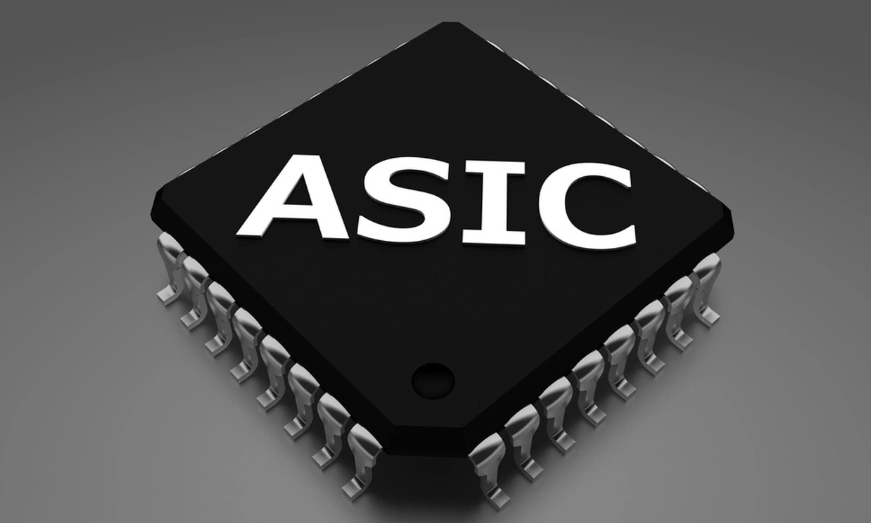
| Microprocessor (MPU)/ASIC | Definition: Complex ICs possessing logic, control, and data processing capabilities. | Power Consumption; RθJC; I/O interface speed (PCIe, DDR). | Determines the complexity of PCB layer count, thermal design, and the Power Delivery Network (PDN). |
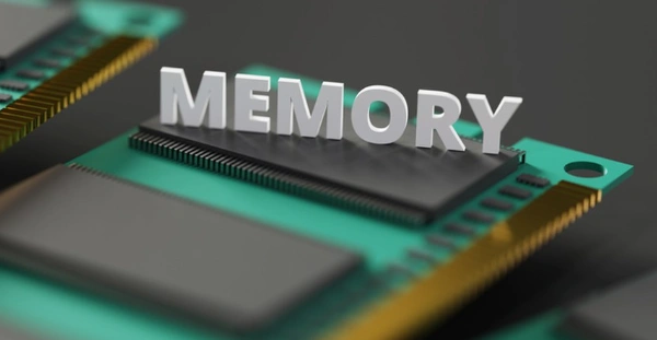
| Memory | Definition: ICs used for storing data and programs (e.g., DRAM, SRAM, NAND Flash). | Data Rate, Density, Access Latency. | High-speed memory (e.g., HBM) requires High-Density Interconnect (HDI) and precise routing strategies. |
| Power Management IC (PMIC) | Definition: ICs specialized in managing and distributing system power, including DC/DC converters and LDOs. | Conversion Efficiency; Transient Response Speed; Package Thermal Dissipation Capability. | Determines the stability, temperature rise, and energy efficiency of the system power supply. |
>> If you want to dive deeper into the classification of electronic components, especially the differences between active and passive components, check out our detailed article: Active vs Passive Electronic Components: A Detailed Comparison, which explains their roles and applications in circuit design.
2.3 Electromechanical/Optoelectronic Components: Interface, Connection, and Human-Machine Interaction
2.3.1 Connectors
Definition and Description: The connector is an electromechanical component, acting like the circuit's "socket" and "plug." Its main purpose is to provide a removable, reusable electrical/signal path between two independent electronic subsystems, devices, or PCBs. It ensures signal continuity while allowing devices to be conveniently connected or disconnected for maintenance, upgrades, or modular design. In high-frequency applications, the connector is not just a physical connection; its impedance matching and shielding performance directly determine signal integrity.
| Specific Type | Definition/Description | PCB Engineer Key Parameters | Design Considerations |
|---|---|---|---|
| Board-to-Board Connector | Definition: Used to transmit signals and power between two PCBs. | Insertion Cycle Life; Contact Resistance; Signal Bandwidth. | High-speed connectors require impedance matching; mechanical installation and shock resistance must be considered. |
| I/O Interface Connector | Definition: Physical connection port for external interfaces (e.g., USB, HDMI, Ethernet). | Shielding Effectiveness; Voltage/Current Rating; Standard Compliance. | Ensure good EMC shielding and grounding design. |
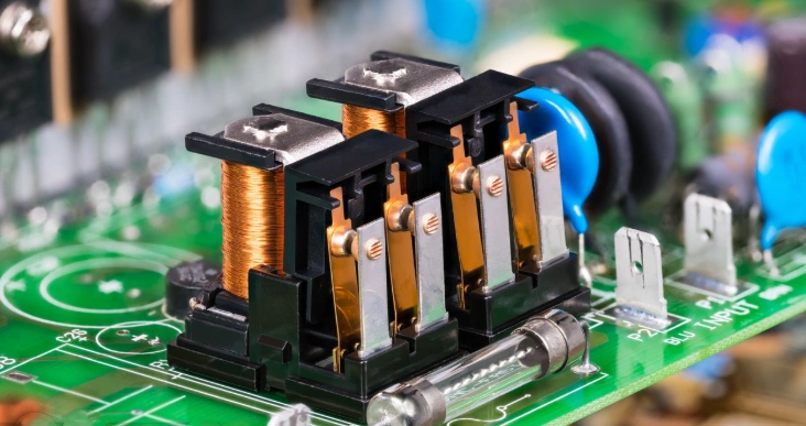
| Relay/Switch | Definition: Relays are electrically controlled switches, using a small current signal to control the physical connection or disconnection of a large current circuit, enabling isolation and control. Switches change circuit status via mechanical operation. | Rated Contact Voltage/Current; Contact Life (cycles); Isolation Voltage. | Must allow sufficient creepage and clearance distances; switch selection requires consideration of mechanical and environmental sealing. |
2.3.2 Sensors
Definition and Description: A sensor is a device capable of detecting a physical input (such as light, heat, motion, pressure, humidity, chemical composition, etc.) and converting it into a measurable, processable electrical signal output. It acts as the "sense organ" for the electronic system to perceive the external world. A sensor typically consists of a sensitive element and signal processing circuitry, converting non-electrical physical quantities into voltage or current signals for subsequent analysis and decision-making by microcontrollers or processors.
| Specific Type | Definition/Description | PCB Engineer Key Parameters | Design Considerations |
|---|---|---|---|
| MEMS Sensor | Definition: Sensors manufactured using Micro-Electro-Mechanical Systems technology (e.g., gyroscopes, accelerometers). | Sensitivity; Resolution; Noise Density. | Routing must be kept away from noise sources; susceptible to mechanical vibration and temperature effects. |
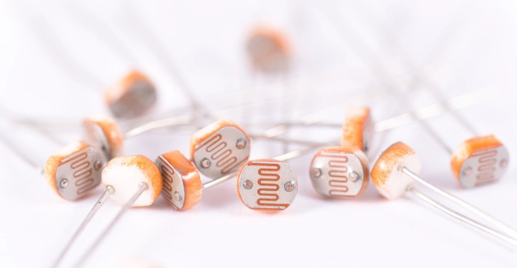
| Optical Sensor | Definition: Devices used to detect light intensity, distance, or perform imaging (e.g., CMOS/Lidar). | Wavelength Range; Accuracy; Sampling Rate. | Lidar demand is growing rapidly in automotive and robotics; careful attention to optical path design and protection is necessary. |
2.3.3 Optoelectronic and Display Components
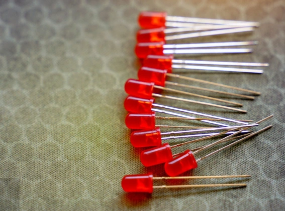
Definition and Description: Optoelectronic and display components are devices that perform energy or information conversion using photoelectric or electro-optic effects, serving as the visual interface for electronic systems to interact with humans or the external environment. These components can convert electrical energy into light energy (like LEDs), convert light energy into electrical energy (like photodiodes), or be used to display information (like OLED/LCDs).
| Specific Type | Definition/Description | PCB Engineer Key Parameters | Design Consideration |
|---|---|---|---|
| Light Emitting Diode (LED) | Definition: A semiconductor diode that converts electrical energy into light energy. | Wavelength (color); Luminous Intensity; Forward Voltage (Vfwd). | High-current LEDs require thermal sink design; driver circuitry and current-limiting resistors must be designed. |
| Display | Definition: Panels used to display images or information (e.g., OLED, LCD). | Resolution; Brightness; Contrast Ratio; Refresh Rate. | Flexible displays impose ultra-thin requirements on FPCs and connectors. |
III. Conclusion: Future Challenges and Skill Requirements for Engineers
The future of the electronic component industry will continue to center on "new devices, new materials, and new processes".
> Recommend reading: Wearable Electronic Components: From Trackers to Wrist-Worn Micro-Computers
3.1 Core Design Skill Upgrade: From Component to System
Faced with the component performance leap (such as the ultra-high-speed switching brought by GaN/SiC), engineers must adopt a system-level mindset that goes beyond basic component selection:
- PI/SI Expertise: Must be proficient in accurately modeling and optimizing component parasitic parameters and their impact on high-speed signal and power delivery networks.
- Thermal Management Practicality: Master the handling of concentrated heat flux from high-power density components (such as GaN FETs and high-performance ASICs), including utilizing RθJC for thermal path design and employing thermal via arrays.
- Reliability Design: Thoroughly understand and apply automotive-grade (AEC-Q) and industrial-grade standards to ensure components operate stably over the long term in extreme environments.
3.2 Conclusion and NextPCB Promotion: Transforming High-Performance Design into Reliable Products
Successful hardware design relies on a deep understanding and precise control of component physical parameters. Proactively embracing the technological revolution brought by third-generation semiconductor materials (GaN/SiC) and mastering the design strategies to manage their extreme performance are fundamental to establishing the next generation of high-efficiency, high-reliability systems.
In this process, transforming complex design concepts and high-performance components into manufacturable, highly reliable physical PCBs, is the final challenge for engineers. NextPCB, as a supplier specializing in high-precision, high-reliability PCB manufacturing and one-stop Electronic Manufacturing Services (EMS), is positioned to be a powerful aid in overcoming the following design challenges:
- Addressing High-Frequency/HDI Needs: This article emphasizes the stringent requirements of high-speed interconnects and Chiplet architectures on high-density interconnect (HDI) PCB materials and processes. NextPCB offers mature HDI manufacturing capabilities and advanced stacking technology to ensure the integrity of high-speed signal routing and minimal signal loss.
- Supporting New Material Applications: Whether dealing with the concentrated heat flux generated by GaN/SiC devices or meeting the demands of automotive electronics for high-Tg, high-reliability substrates, NextPCB provides customized thermal solutions and supports high-grade materials, ensuring the long-term stable operation of power modules. >Visit advanced pcb material library: Advanced PCB Materials, Manufacturing & Assembly | NextPCB
- One-Stop Solution for Reduced Supply Chain Risk: Beyond high-quality PCB fabrication, NextPCB offers comprehensive component sourcing and assembly services. This allows engineers to focus on design optimization, delegating complex supply chain tasks—such as component procurement, authenticity verification, and precision placement (like BGA, high-density SMT)—to a professional manufacturing partner, thus effectively reducing project risk and accelerating time-to-market.
By combining your specialized design knowledge with NextPCB's high-precision manufacturing capabilities, you can ensure your next-generation electronic product achieves industry-leading levels in performance, thermal management, and overall reliability.

