NextPCB Capabilities
Printed Circuit Boards
NextPCB Capabilities
Printed Circuit Boards
 PCB Assembly
 Layer Buildup
 SMD-Stencils
 PCB Design-Aid & Layout
 Mechanics
 Quality
 Drills & Throughplating
 Factory & Certificate
 PCB Assembly Factory Show
Certificate
PCB Assembly Factory Show
Certificate
Support Team
Feedback:
support@nextpcb.com


Semiconductors play a vital role in countless electronic devices and could be called the heart of modern electronics.
They form the foundation for transistors, diodes, and integrated circuits that are essential components from smartphones to computers.
In the world of semiconductors, two fundamental types stand out namely P-type and N-type.
In this article, we will explore the characteristics, differences, and significance of P-type and N-type semiconductors in detail.
Introduction
Semiconductors are materials that have electrical conductivity in between that of conductors and insulators. The behavior of semiconductors is dependent on the presence of charge carriers.
Charge carriers are known to be electrons or holes (electron deficiencies)
P and N-type semiconductors represent two sides of this electrical phenomenon.
Now we will go into detail about the P-type and N-type semiconductors.
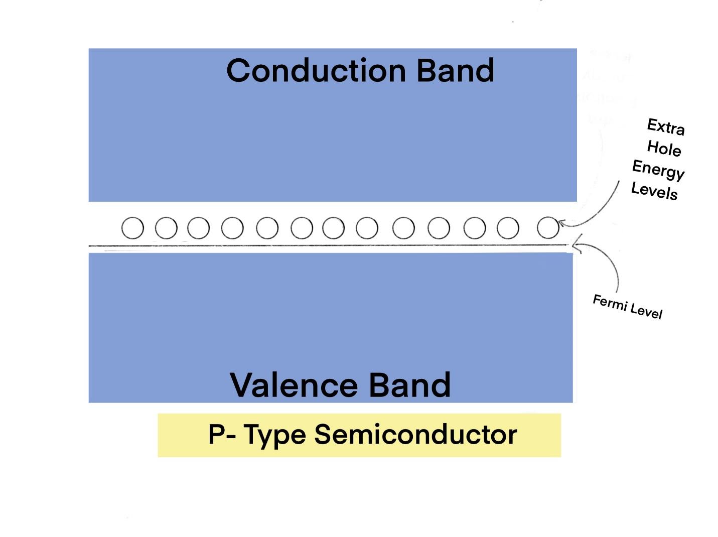
What is a P-type Semiconductor?
Characteristics
P-type semiconductors are materials doped with certain elements to create an excess of "holes" in the crystal lattice.
Now you may think what is doping? Doping is nothing but adding elements depending on the requirements for enhanced conductivity.
These holes act as positive charge carriers. In P-type semiconductors, the majority of charge carriers are holes, and they play a crucial role in electrical conduction.
Doping Process
To create a P-type semiconductor, a pure semiconductor material such as silicon is doped with specific elements. Boron is one of the most common dopants for P-type semiconductors.
When boron atoms are introduced into the crystal lattice of silicon, they create "holes" in the structure because boron has one less valence electron than silicon. This results in a deficiency of electrons in the material, making it P-type.
Electrical Conductivity
P-type semiconductors have lower electron mobility and lower electrical conductivity compared to N-type semiconductors. This is because holes move less efficiently than electrons in a crystal lattice.
Applications
P-type semiconductors find a wide variety of applications in the world of electronics. They are commonly used in Diodes, Transistors, and solar panels.
Diodes: P-type semiconductors are frequently used in the creation of diodes, which allow current to flow in one direction while blocking it in the opposite direction. This property is essential in rectifying AC signals and converting them into DC.
Transistors: Transistors are the fundamental building blocks of digital logic circuits. They serve as amplifiers and switches, and P-type transistors play a key role in digital logic gates(AND, OR, and NOT gates).
Photovoltaic Devices: P-type semiconductors are utilized in the manufacturing of solar cells. They are responsible for generating electron-hole pairs when exposed to light, thus converting sunlight into electricity.
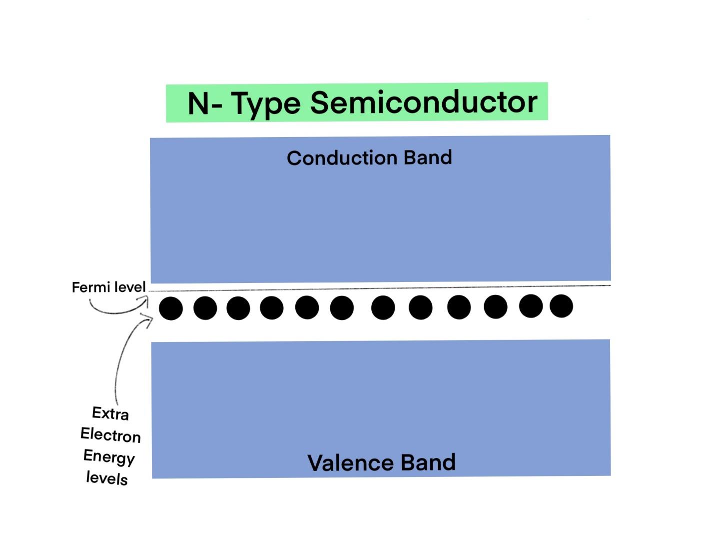
What is N-type Semiconductor?
Characteristics
In contrast to P-type semiconductors, N-type semiconductors are doped with elements like phosphorous or arsenic that introduce an excess of electrons into the crystal lattice. This excess of electrons becomes the majority charge carriers in the material.
Doping Process
Common doping materials or dopants for N-type semiconductors include phosphorus and arsenic, both of which have extra valence electrons(free electrons) compared to the host material (e.g., silicon).
The extra electrons introduced by these dopants significantly increase the electron density in the crystal structure, creating an abundance of negative charge carriers, which are crucial for conduction.
Electrical Conductivity
N-type semiconductors have higher electron mobility and greater electrical conductivity compared to P-type semiconductors. Electrons are more mobile and efficient charge carriers in the crystal lattice.
Applications
N-type semiconductors play a crucial role in the world of electronics, particularly in Integrated circuits, Logic gates, and photodetectors.:
Integrated Circuits: N-type and P-type transistors are combined to create CMOS (Complementary Metal-Oxide-Semiconductor) integrated circuits. N-type transistors are responsible for the "ON" state in CMOS logic gates, allowing current to flow.
Digital Logic Gates: N-type semiconductors are essential components of digital logic gates. They are used in devices like NAND, NOR, and NOT gates, which form the basis of digital electronic systems.
Photodetectors: N-type semiconductors are used in photodetectors and photodiodes. When exposed to light, they produce an excess of electrons, which can be detected as a photocurrent. This property is vital in optical communication and imaging devices.
Difference between P-type Semiconductor and N-type Semiconductor
Whether to choose a p or n-type semiconductor can be decided after considering these factors
Electrical Behavior
The most fundamental difference between P-type and N-type semiconductors is their electrical behavior.
P-type semiconductors conduct electricity mainly through the movement of "holes" (positive charge carriers), whereas N-type semiconductors primarily use electrons (negative charge carriers) for conduction.
Doping
P-type semiconductors are created by doping a pure semiconductor material with elements that have fewer valence electrons than the host material, leading to a deficit of electrons.
N-type semiconductors, on the other hand, are formed by doping with elements that have more valence electrons, creating an excess of electrons.
Majority Charge Carriers
In P-type semiconductors, the majority of charge carriers are holes (positive charges), whereas in N-type semiconductors, the majority of charge carriers are electrons (negative charges).
Electrical Conductivity
P-type semiconductors have lower electron mobility and lower electrical conductivity compared to N-type semiconductors. This is because holes move less efficiently than electrons in a crystal lattice.
Application
The choice between P-type and N-type semiconductors depends on the desired functionality in electronic devices. P-type semiconductors are often used in diodes and transistors, while N-type semiconductors are crucial in the formation of logic gates and other electronic components.
Manufacturing Methods
Let us now understand how the P-type and N-type semiconductors are manufactured which is essential to know their properties fully.
P-type Semiconductor Manufacturing
The manufacturing process of P-type semiconductors begins with a base semiconductor material, typically silicon.
To create a P-type semiconductor, a precise amount of a dopant, such as boron, is introduced during the crystal growth process. This is done by doping the material, which means adding a small quantity of the dopant element to the silicon melt before it solidifies. The boron atoms take the place of some silicon atoms in the crystal lattice, creating "holes" where there is a deficiency of electrons.
N-type Semiconductor Manufacturing
The manufacturing of N-type semiconductors follows a similar process, using a different dopant. For N-type semiconductors, elements like phosphorus or arsenic are introduced into the silicon crystal during the growth process. These dopants have extra valence electrons compared to silicon, and when they take the place of silicon atoms in the crystal lattice, they introduce an excess of electrons.
The control of the doping process is crucial to the performance of semiconductors. Manufacturers carefully regulate the concentration of dopants to achieve the desired electrical properties. Precision is one of the key factors that enable the production of modern electronic devices.
N-type vs. P-type Semiconductors
Understanding the differences between N-type and P-type semiconductors is necessary to know their effective use in various applications.
The differences can be observed in the following characteristics.
Doping Mechanisms
N-type semiconductors are doped with elements from Group V of the periodic table, which have five valence electrons. These elements provide an extra electron, making the material electron-rich. In simpler words, P-type semiconductors are doped with elements from Group III of the periodic table, which have only three valence electrons, resulting in an electron-deficient material.
Electrical Behavior
Due to the excess of electrons, N-type semiconductors are electron-dominant and exhibit a surplus of negative charge carriers. To summarize, P-type semiconductors rely on holes, or electron deficiencies, for electrical conduction. This fundamental difference in charge carriers results in distinct electrical behaviors.
Mobility
Electron movement/mobility in N-type semiconductors is generally higher than hole mobility in P-type semiconductors. Electrons move more efficiently in a crystal lattice, which contributes to the higher electrical conductivity of N-type materials.
Applications
The choice of the type of semiconductor used in a particular application is based on the desired electrical characteristics and functionality of the device.
Doping the N-type and P-type
Like I said earlier the process of introducing dopants to create N-type and P-type semiconductors is called doping. Doping is a precise and controlled procedure used in semiconductor manufacturing.
N-type Doping
To create N-type semiconductors, Group V elements are introduced as dopants. Phosphorus and arsenic are common dopants used in N-type doping. When these elements are introduced into the silicon crystal lattice during the manufacturing process, they bring in extra electrons. This results in the formation of an N-type semiconductor with an excess of negatively charged electrons.
P-type Doping
For P-type doping, elements from Group III are employed. Boron is a common dopant used for P-type semiconductors. Boron has one less valence electron than silicon, which leads to the creation of "holes" where electrons are deficient. These holes serve as positive charge carriers, making the material P-type.
Importance of Controlled Doping
The concentration and distribution of dopants in the crystal lattice are critically controlled during the manufacturing process. The precise regulation of dopants determines the electrical properties of the resulting semiconductor material. This level of control allows for the customization of semiconductors to meet the specific requirements of various electronic components.
P-type and N-type Semiconductors in Electronic Devices
P-type and N-type semiconductors are at the core of nearly all electronic devices. Their unique electrical properties and behavior are harnessed in various ways to perform specific functions in electronic components.
Transistors
Transistors are among the most fundamental electronic components, and they rely heavily on both N-type and P-type semiconductors. Bipolar junction transistors (BJTs) are constructed using both NPN (N-type, P-type, N-type) and PNP (P-type, N-type, P-type) configurations.
In these transistors, the behavior of N-type and P-type materials controls the flow of current, which amplifies and switches electronic signals. Field-effect transistors (FETs), including metal-oxide-semiconductor FETs (MOSFETs) and junction FETs (JFETs), also utilize N-type and P-type materials for their operation.
Diodes
Diodes are semiconductor devices with P-N junctions, where a P-type material is in contact with an N-type material. This junction allows current to flow in one direction while blocking it in the other. P-N junction diodes find extensive use in rectification, signal clipping, and voltage regulation.
Integrated Circuits (ICs)
Integrated circuits are composed of a multitude of transistors, diodes, and other electronic components. These components are made using P-type and N-type semiconductors, forming complex electronic circuits with a range of functionalities. CMOS (Complementary Metal-Oxide-Semiconductor) ICs, for example, use both P-type and N-type transistors to create logic gates and memory cells.
Photovoltaic Devices
Solar cells are made using both P-type and N-type semiconductors. When exposed to sunlight, the P-N junction in these cells generates an electric current by facilitating the movement of electrons from the N-type region to the P-type region. This electrical energy is then harnessed for various applications, particularly for generating electricity in solar panels.
N-type vs. P-type Semiconductor: Key Applications
The choice between N-type and P-type semiconductors is determined by the specific requirements of an application. Here are some key applications where the distinction between N-type and P-type materials is crucial:
Digital Logic Circuits
Digital logic gates are the building blocks of digital electronics. N-type and P-type transistors are combined to create CMOS (Complementary Metal-Oxide-Semiconductor) logic gates. N-type transistors conduct when a logical "1" is applied, allowing current to flow from the power supply to the output. P-type transistors conduct when a logical "0" is applied, allowing current to flow from the power supply to the output. This combination forms the basis for digital logic circuits and microprocessors.
Photodetectors and Imaging Devices
N-type semiconductors, particularly silicon, are widely used in photodetectors and imaging devices. When light strikes an N-type region, it generates an excess of electrons, leading to a measurable current or voltage. This property is essential in applications such as digital cameras, solar cells, and optical communication systems.
Solar Cells
Solar cells are made by creating a P-N junction, where one side is P-type and the other is N-type. When exposed to sunlight, the P-N junction generates an electric current as photons strike the semiconductor material, releasing electrons. This current is then harvested as electrical energy and is the basis for solar power generation.
Amplifiers and Oscillators
In electronic circuits such as amplifiers and oscillators, transistors play a significant role. Amplifiers use NPN or PNP transistors to control the flow of current, amplifying signals. Oscillators, which produce continuous.
- What's the difference between MOSFET and BJT and how to choose?
- Autumn Offer: Get $30 off PCB orders over $100 with NextPCB
Still, need help? Contact Us: support@nextpcb.com
Need a PCB or PCBA quote? Quote now


 Surface