

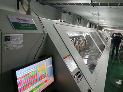
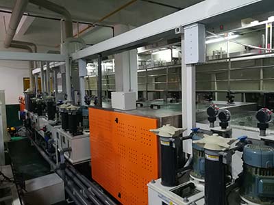
 NextPCB Capabilities
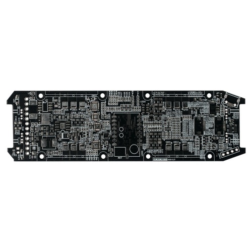
 PCB Assembly
 Layer Buildup
 SMD-Stencils
 PCB Design-Aid & Layout
 Mechanics
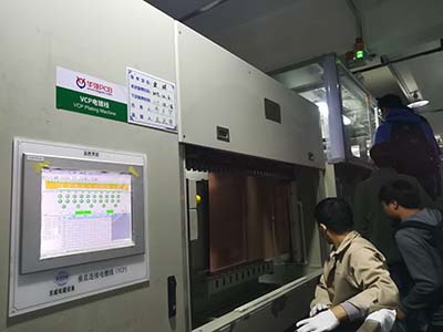
 Surface
 Quality
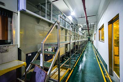
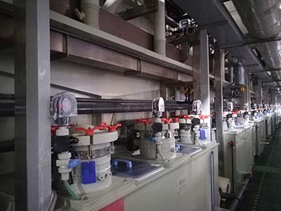
 Drills & Throughplating
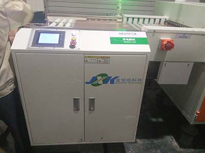
 Factory & Certificate


Categories
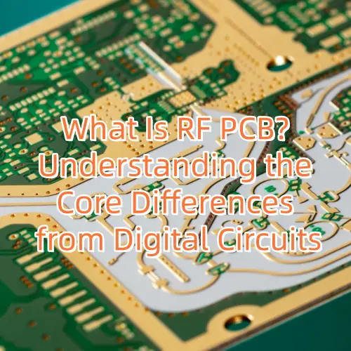
Recommended Article:
- 112G PAM4 PCB Design for AI Servers: Material Selection, Trace Routing and SI Rules
- PCIe Gen5 PCB Design Guidelines: Impedance, Loss Budget & Via Optimization
- Why AI GPUs Require 30+ Layer HDI PCBs
- How GPU PCBs Are Manufactured: From Bare Board to Final PCBA
- AI Accelerator PCB Design Guide: Layers, Materials and Signal Integrity for H100/H200 Boards
- How to Speed Up Hardware Prototype Bring-up: An Engineer's Guide
- AI Training vs AI Inference: Why They Need Different PCB Designs
- H100 vs MI300X: NVIDIA vs AMD AI Accelerator Comparison
- What Is an OAM Module? Open Accelerator Module Standard for AI Hardware
- What Is NVSwitch? The Silicon Behind NVIDIA's GPU Cluster Scale-Out