
 Surface


Stacy Lu

 NextPCB Capabilities
Printed Circuit Boards
NextPCB Capabilities
Printed Circuit Boards
 PCB Assembly
 Layer Buildup
 SMD-Stencils
 PCB Design-Aid & Layout
 Mechanics
 Quality
 Drills & Throughplating
 Factory & Certificate
 PCB Assembly Factory Show
Certificate
PCB Assembly Factory Show
Certificate
Support Team
Feedback:
support@nextpcb.com


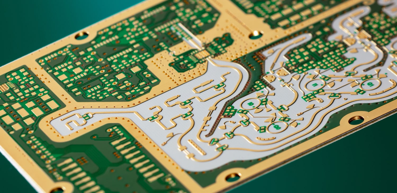
In the design of radio frequency (RF) and microwave circuits, Rogers RO4350B (also written as Rogers 4350B) high-frequency PCB material is almost an unavoidable choice. It is widely used in scenarios such as communication base stations, millimeter-wave radar, RF front-end modules, power amplifiers, and antenna feed networks.
In the experience of PCB manufacturing and engineering support, we have seen too many RF designs encounter significant deviations during the prototype phase: issues arise not only from inconsistencies between simulation and actual measurement but also from uncontrolled impedance, board warping, excessive insertion loss, and even complete design rejections.
The problem often lies not in "design capability", but in insufficient understanding of the characteristics of RO4350B material and manufacturing boundaries.
This article will systematically clarify the key points and common pitfalls in the prototype production of RO4350B high-frequency PCBs from an engineering and manufacturing perspective, helping RF designers minimize risks during the prototyping phase.
>> Browse NextPCB Rogers Manufacturing Capabilities ↓Rogers RO4350B Datasheet Download
Even with the continuous emergence of new high-frequency materials in the market, RO4350B maintains significant comprehensive advantages during the prototyping and small to medium batch stages, primarily reflected in the following three aspects.
1. Stable and Predictable Electrical Performance (of Greatest Concern to RF Design)
The dielectric constant (Dk) of RO4350B remains stable at:
Dk = 3.48 ± 0.05
For RF and microwave circuits, the stability of Dk is more important than its "absolute value." Even a 0.1 variation can lead to:
RO4350B demonstrates high consistency across the 1GHz–20GHz frequency range, making it highly suitable as a material for RF prototype validation.
2. Processing Similar to FR-4, Significantly Reducing Prototype Delivery Time
Unlike traditional PTFE (Teflon) high-frequency materials:
What does this mean?
For the development phase, this presents an extremely practical advantage of RO4350B.
3. Excellent Thermo-Mechanical Reliability, Suitable for Repeated Debugging and Soldering
The Z-axis coefficient of thermal expansion (CTE) of RO4350B is close to that of copper foil, which is particularly critical for the following scenarios:
The results are:
Using incorrect material parameters for simulation in high-frequency PCB prototyping is equivalent to deceiving oneself.
Key Characteristics:
| Property | RO4350B | High-Speed FR-4 (e.g., IT-180A) | Impact on RF Design |
| Dielectric Constant (Dk) | 3.48 | 4.2 – 4.5 | Determines impedance, trace width, and phase delay |
| Loss Factor (Df) | 0.0037 @ 10GHz | 0.015 – 0.020 | Determines insertion loss and link budget |
| Thermal Conductivity | 0.62 W/m·K | 0.25 – 0.30 | Affects heat dissipation in PAs and power devices |
| Water Absorption Rate | 0.06% | 0.10% – 0.20% | Impacts long-term stability and consistency |
One detail the table above doesn’t make obvious: 3.48 is RO4350B’s process Dk — the value measured on a test coupon per IPC-TM-650 2.5.5.5. For actual impedance calculations on microstrip or stripline structures, Rogers recommends using the design Dk of 3.66 instead. Plugging 3.48 directly into a field solver is one of the more common reasons prototype impedance comes back several ohms off target — if your 50Ω microstrip is testing low, this is usually why.
The conclusion is straightforward:
To control costs, hybrid stack-ups using RO4350B + FR-4 are quite common, such as:
The problem: The CTE and thermal shrinkage behavior of the two materials are completely different.
Engineering Recommendations:
Otherwise, severe warping may occur after hot air leveling (HASL) or reflow soldering.
In RO4350B high-frequency prototypes, the sources of impedance control error extend beyond just trace width:
Engineering Recommendations:
Clearly specify in the Gerber/Fabrication Note:
This enables PCB engineers to accurately compensate based on actual stack-up and copper thickness.
ENIG (Electroless Nickel Immersion Gold)
Immersion Silver
Engineering Recommendations:
Common thicknesses include:
Not having stock can directly increase the delivery time by an additional 3 to 5 days.
A common question at this stage is how wide a 50Ω microstrip trace needs to be on 10 mil, 20 mil, or 60 mil (1.524mm) RO4350B. There isn’t one universal number — the correct width depends on your exact copper weight, copper roughness, and whether the design Dk (3.66) or process Dk (3.48) was used in the solver, as noted above. Rather than working from a generic lookup table, run your specific stack-up through NextPCB's impedance calculator, or request an engineering review before you release Gerbers.
A high-quality engineering document should include:
This ensures engineering confirmation (EQ) is typically completed within 2 hours.
Rogers materials are expensive, so maximizing utilization is crucial:
This is especially important during the prototype phase.
RO4350B high-frequency PCB prototyping is not just about "producing a board"; it is about:
Choosing a manufacturing partner like NextPCB that truly understands Rogers materials, high-frequency processes, and RF design logic is often more decisive for project success than merely comparing prices.
If you are engaged in RO4350B stack-up design, impedance calculations, or high-frequency prototype evaluations, feel free to connect directly with our engineering team. With 15 years of frontline experience, we specialize in serving RF design needs.
Here are some of the most commonly asked questions during the project evaluation phase:
Q1: What is the difference between RO4350B and RO4350?
The vast majority of materials available today are RO4350B. It is a flame-retardant (FR) upgraded version of the original RO4350. Both have nearly identical electrical performance, but RO4350B meets the UL 94 V-0 standard, which is the current industry standard. You may also see this material written as "Rogers 4350B" rather than "RO4350B" — both names refer to the same laminate.
Q2: What type of copper foil should be used with RO4350B in prototype design?
For high-frequency applications, we strongly recommend using low-roughness copper foil (Low Profile Copper). While electrolytic copper (ED Copper) is commonly used, if your frequency exceeds 20GHz, choosing rolled copper or low-roughness copper foil can significantly reduce conductor losses.
Q3: Why do my RO4350B impedance test results have a 2-3 ohm deviation from simulations?
This is typically caused by three factors: actual substrate thickness tolerances, dielectric loss after lamination, and insufficient etch compensation. During the prototyping phase, it's advisable to include test coupons in the Gerber files, which we will use as the final standard for impedance calibration.
Q4: Can I perform manual soldering on RO4350B prototypes?
Absolutely. RO4350B has a very high glass transition temperature (Tg > 280°C), which provides significantly better thermal resistance than FR-4. However, due to its faster heat conduction, we recommend using a slightly higher wattage soldering iron and controlling the soldering time to protect pads.
More Advanced PCB Manufacturing Capabilities at NextPCB Instant Ro4350B PCBs Quote & Order Online

Still, need help? Contact Us: support@nextpcb.com
Need a PCB or PCBA quote? Quote now

