
 NextPCB Capabilities
Printed Circuit Boards
NextPCB Capabilities
Printed Circuit Boards
 PCB Assembly
 Layer Buildup
 SMD-Stencils
 PCB Design-Aid & Layout
 Mechanics
 Quality
 Drills & Throughplating
 Factory & Certificate
 PCB Assembly Factory Show
Certificate
PCB Assembly Factory Show
Certificate
Support Team
Feedback:
support@nextpcb.com


In modern wireless communication systems—especially as we transition through 5G-Advanced and look toward the dawn of 6G in 2026—the hardware architecture is almost universally divided into two main domains: radio frequency (RF) circuits and digital circuits. While they work together to transmit and receive data (often ranging from Mbps to multi-Gbps), their physical appearance, design methodologies, and underlying physics are fundamentally different.
To build reliable wireless devices, engineers must understand what is RF PCB, how it contrasts with standard digital circuit boards, and why specific design rules dictate its success.
An RF PCB (Radio Frequency Printed Circuit Board) is a specialized type of high-frequency PCB designed to handle signals operating in the RF spectrum, generally ranging from several Megahertz (MHz) up to Gigahertz (GHz), and increasingly into the sub-Terahertz (Sub-THz) ranges.
Unlike standard digital boards that merely connect components to process binary states, an RF PCB functions as an active component within the system. The physical layout, trace dimensions, and substrate materials directly impact electromagnetic wave propagation. In an RF PCB, the transmission lines are not just wires; they are conduits for power transfer where concepts like return path, grounding, and electromagnetic interference (EMI) play critical roles in overall system performance.
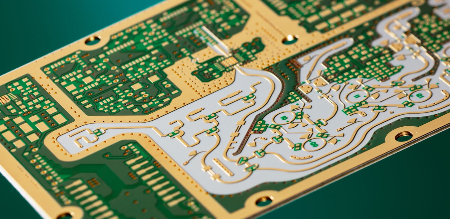
A typical RF PCB showcasing specialized trace geometries and grounding techniques for 2026-standard wireless systems.
Before diving deep into the specifics, the table below summarizes the fundamental differences between RF and digital circuits based on traditional design parameters:
| Parameter | RF Circuits | Digital Circuits |
|---|---|---|
| Operating Impedance | Typically low (50Ω standard) | Low-speed: High (>10kΩ) High-speed: Lower, approaches RF |
| Impedance Matching | Strictly required for input/output | Low-speed: Not required High-speed: Strictly required |
| Operating Current | Milliampere (mA) level (for power transfer) | Low-speed: Microampere (μA) level High-speed: mA level |
| Transmission Nature | Power transmission | State transmission (Logic 0s and 1s) |
| Signal Spectrum | Narrow (typically Sine waves) | Broad (Square wave pulses with harmonics) |
| PCB Layout Focus | EMI, crosstalk, precise trace geometries | Low-speed: Basic connectivity High-speed: Signal integrity (RF-like) |
| Design Methodology | Frequency domain simulation | Time domain simulation |
| Testing Instruments | Spectrum/Network analyzers (dBm, dBW) | Oscilloscopes, Logic analyzers (dBV) |
A primary distinction lies in what the signals represent. A digital circuit transmits states (0s and 1s) using square wave pulses. Its primary concern is maintaining the correct logic state with minimal power consumption. Because square waves are composed of fundamental frequencies and multiple harmonics, digital signals inherently possess a very broad spectrum.
In contrast, an RF circuit is designed for power transmission. RF signals are typically sine waves, resulting in a relatively narrow spectrum. The goal is to transfer the RF signal's power from a source to a load as efficiently as possible.
Digital circuits are categorized by data transmission rates (bps, Mbps, Gbps), whereas RF circuits are defined by continuous wave frequencies (Hz, MHz, GHz).
Using the modulator/demodulator as a boundary, digital and RF circuits reside on opposite sides.
As of 2026, the demands on RF PCBs have evolved dramatically to support next-generation communications:
In practical RF PCB design, engineers must carefully control several key layout factors to ensure performance:
Of all the differences and modern challenges mentioned above, the most critical parameter that dictates the success or failure of an RF PCB remains impedance matching.
In low-speed digital circuits, impedance matching is largely ignored. But in the RF domain, the input impedance must perfectly match the signal source, and the output impedance must perfectly match the load. Because RF circuits are designed to transmit power, any mismatch along the transmission line results in signal reflection. This reflection not only degrades the signal integrity but can also damage sensitive transmitter amplifiers.
When high-speed digital data rates reach RF frequencies, they too require strict impedance matching to prevent signal attenuation, jitter, and reflection. To achieve this level of precision, engineers rely on professional tools and services. You can accurately calculate your trace parameters using a PCB impedance calculator or consult professional impedance control stackups. For complex designs requiring high-frequency materials and precision manufacturing, getting an advanced PCB quote is the first step toward a successful build.
Understanding that every trace on an RF PCB behaves as an active transmission line leads us directly into the intricacies of RF PCB impedance matching.
RF PCB manufacturing requires precise impedance control and validated stackup configurations. Use NextPCB's Multilayer Stackup Tool to select your layer count, material, and get a certified impedance-controlled build.
Still, need help? Contact Us: support@nextpcb.com
Need a PCB or PCBA quote? Quote now


 Surface

