
 Surface


(containing copper traces), solder mask layers, silkscreen and board outline. A two-layer board requires around 7 files in Gerber format and an NC drill file, often in Excellon format to produce a PCB.

 NextPCB Capabilities
Printed Circuit Boards
NextPCB Capabilities
Printed Circuit Boards
 PCB Assembly
 Layer Buildup
 SMD-Stencils
 PCB Design-Aid & Layout
 Mechanics
 Quality
 Drills & Throughplating
 Factory & Certificate
 PCB Assembly Factory Show
Certificate
PCB Assembly Factory Show
Certificate
Support Team
Feedback:
support@nextpcb.com


This article is available in e-book format. Download the PDF here!
Electronics manufacturing can be a daunting yet fascinating field. The penetration of electronics in every aspect of life - from complex circuit boards in everyday devices to sophisticated PCB assembly processes - is a testament to the technological advancements made over the past half-century, which have only recently become more accessible to non-experts.
In the past decade, the industry has transformed with new players like NextPCB in Asia offering highly competitive and affordable quickturn manufacturing services and one-stop-shop solutions to international markets, removing major obstacles for hobbyist circles and small-scale businesses while providing more flexibility compared to their traditional counterparts.
This rapid globalization of electronics manufacturing has enabled the emergence of new techniques and approaches and opened doors to new customers who need to get up to speed quickly in the highly competitive electronics market.
There is no shortage of resources available but bite-sized chunks of information from disparate sources of varying quality and age can lead to conflicting information and a fragmented understanding. This guide aims to make sense of it all by bringing you up to date with common PCB assembly services terminology, PCB basics and PCB assembly processes that go into producing electronic hardware and the considerations that go into making cost-effective, producible and reliable electronics in today’s fast-paced industry.
Printed Circuit Board Assembly, sometimes abbreviated to PCBA, describes the process of populating the bare circuit board with electronic components, including the formation of solder joints and subsequent testing and inspection procedures. The abbreviation PCBA can also describe the populated device, i.e. PCB assembled. So 5 PCBA would be 5 assembled PCB devices. PCBA also typically refers to the populated circuit board without the enclosure or mechanical parts. Understanding pcb assembly meaning is essential for distinguishing between bare PCBs and fully assembled boards in manufacturing workflows.
Bare PCB on the left and populated PCB with components on the right
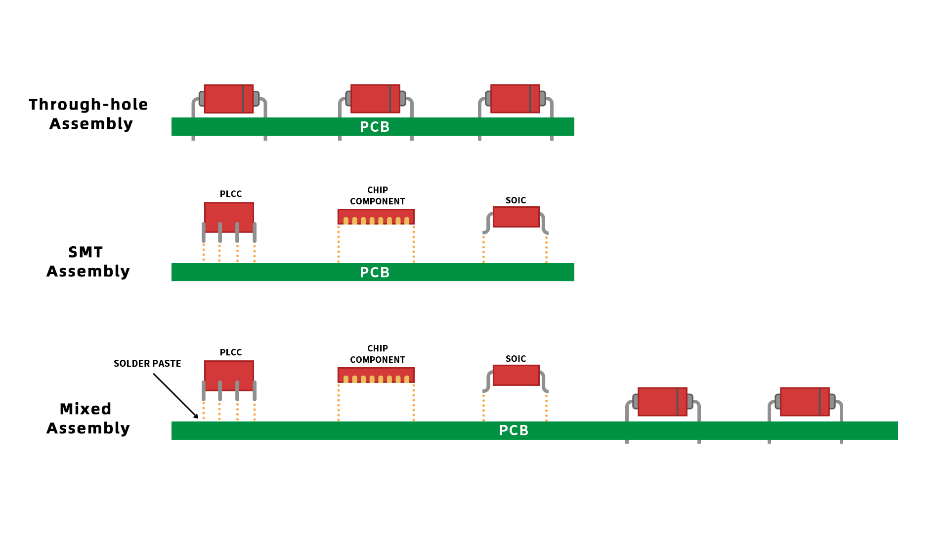
PCBA devices and processes can be labeled according to how the boards are to be assembled, the number of sides, and the types of parts to be populated onto the board etc. These labels can indicate to manufacturers how assembly should be approached and can have significant influence on cost and production difficulty, which in turn influences design decisions.
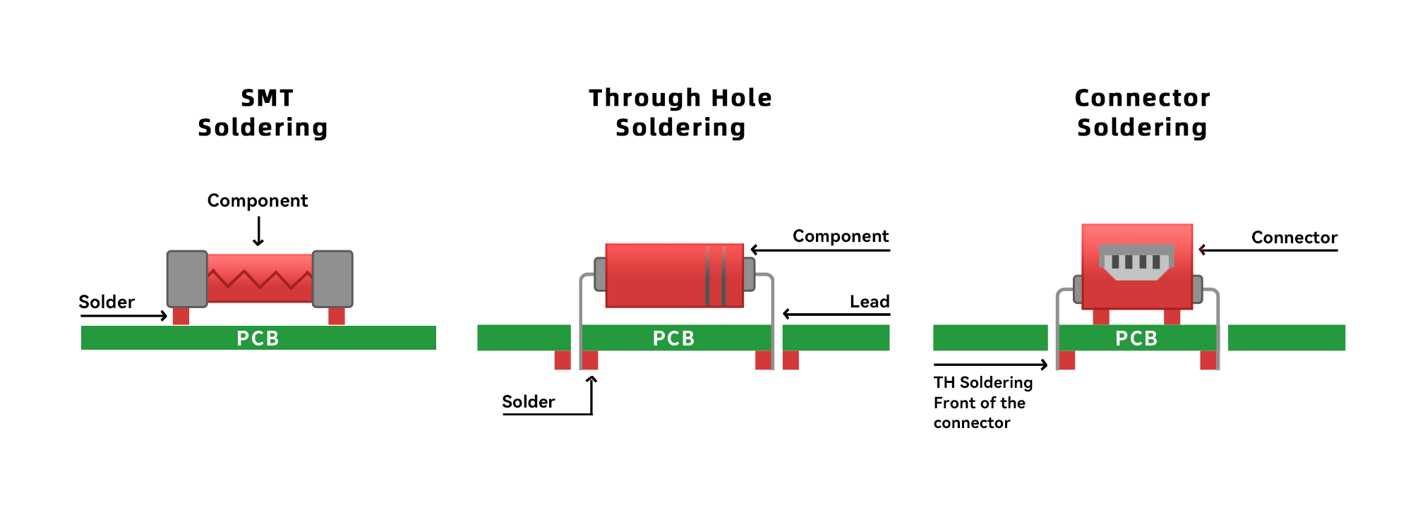
This refers to the types of components destined to be soldered onto the boards. As the name suggests, through-hole parts have long leads that go through the boards through plated through-holes (PTH). Molten solder is then applied to the opposite side or both sides to hold the part in place.
Surface mount components have metallic contacts that are attached to solder pads situated on the surface of the boards.
A circuit board that only has through-hole devices (THD) or surface mount devices (SMD) can be called a through-hole board or surface mount board, respectively.
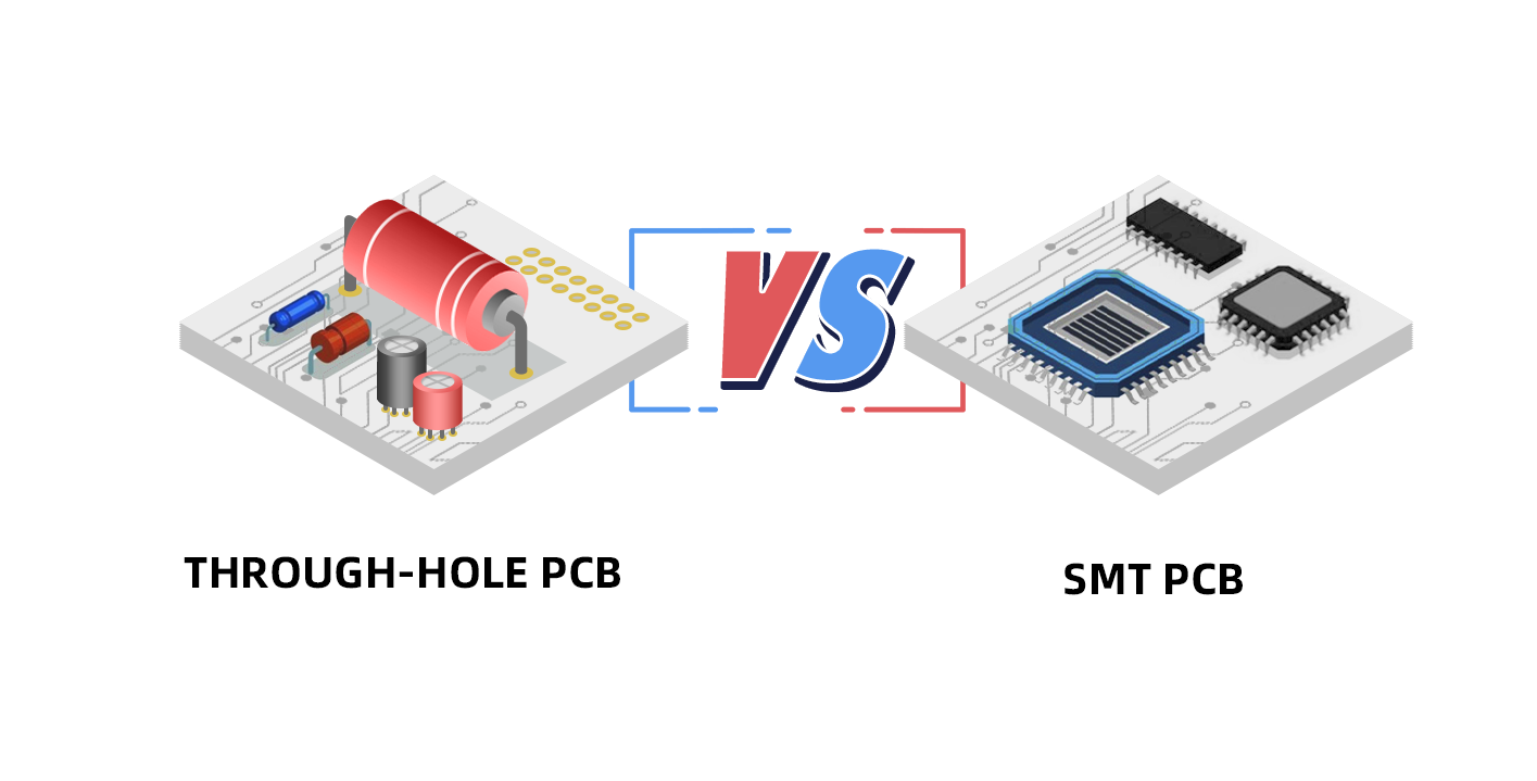
Nowadays, most devices have a combination of both types of components to make the most of their advantages. Such boards are referred to as mixed assembly boards. This integration of technologies is a key part of the modern printed circuit board components assembly process.
The following acronyms are often used to label processes, parts and designs:
Single and double-sided refers to the number of assembly sides required to complete a PCBA. A single-sided PCBA is a design where components are only located on one side whereas for double-sided PCBA, components are soldered to both top and bottom sides. For both surface mount and through-hole boards, double-sided assembly increases production complexity.
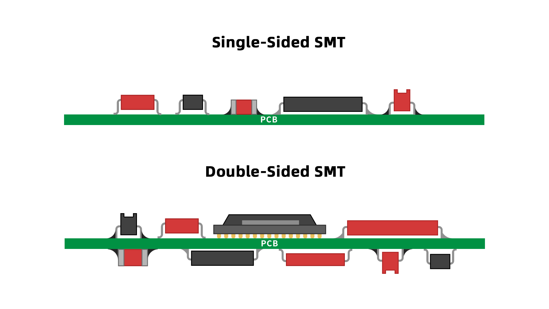
For example, double-sided surface mount boards that undergo soldering in a reflow oven require two passes, one for each side. Often, the side with fewer or lighter components are populated first, then the boards are flipped over and the process is repeated. This helps prevent heavier parts from detaching during the second pass. Custom trays and/or glue may also be used to hold heavier parts in place, being critical in the overall pcb assembly process to ensure consistent quality across both sides of the board.
This refers to how the boards are assembled and has a strong influence on the cost-benefit ratio. PCBA boards can be manually assembled, assembled using automated machines, or by using a combination of manual and automated methods, each of which has its advantages and disadvantages.
Manual Assembly
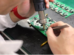
Manually assembled or hand-soldered boards are soldered using non-automated means. For through-hole parts and (surface mount parts to some extent), this involves a technician using a soldering iron and coils of solder wire. For surface mount assembly this could mean manual stencil printing and placement of parts before being placed into a reflow oven.
Manual assembly can be beneficial for prototype orders where only a handful of pieces are required. Automated equipment often requires setup or programming that is specific to the design which may not be worthwhile for small orders.
Automated Assembly
Automated assembly in a mass production setting uses a fully connected online assembly line where machines are connected head-to-toe and boards pass on conveyors from one machine to the next. This sophisticated pcb assembly line set-up requires minimum supervision and can be left running over long periods, but set-up and ironing out problems take up a substantial amount of time and resources. Small batch or agile operations can be semi-automated to facilitate flexibility, which is necessary to cater to a high volume of small orders.
Automated assembly of through-hole parts could involve an automated insertion machine before passing through a wave soldering machine. Surface mount parts can be placed on PCB boards at high speed and accuracy with the help of pick-and-place machines.
|
|
Manual Soldering |
Automated Soldering |
|
Advantages |
|
|
|
Disadvantages |
|
|
Advantages and disadvantages of manual and automated assembly methods
Contract manufacturers often offer complete turnkey manufacturing solutions to their clients. Turnkey PCBA involves taking the client’s design documentation and taking care of the procurement of all materials and manufacturing, including the manufacture of the bare PCBs. Turnkey service providers often also provide other EMS (Electronic Manufacturing Services) such as electromechanical assembly and firmware burning.
The words turnkey or consignment refer to the procurement of electronic components and bare circuit boards. For consignment projects, the client provides all the materials and the assembly house only takes care of the manufacturing process. Turnkey services streamline the entire printed circuit board assembly process by integrating material procurement, manufacturing, and testing into a single workflow. With turnkey, this is the job of the assembly house. With turnkey PCBA, the client does not need to get involved with the supply chain or have a deep understanding of the manufacturing process.
Another advantage of this is that the assembly house can dictate how to prepare the materials in a way that best suits their operations and machinery.
For example, individual boards often need to be arranged into a panel of several boards. The layout of the panel depends on the assembly house’s equipment and preferences, so leaving this in the hands of the contract manufacturer is preferable unless in special circumstances.
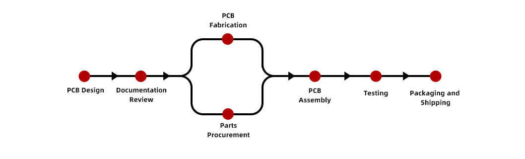
The hardware development cycle involves several key stages from concept to market which includes several manufacturing stages. A turnkey service also includes the procurement of materials required for PCB manufacturing, ensuring all components are available for the assembly process.
Contract manufacturers generally request these 3 pieces of documentation to complete PCB assembly:
Gerber files are the graphical representations of the layers that go into producing the printed circuit board including copper layers
(containing copper traces), solder mask layers, silkscreen and board outline. A two-layer board requires around 7 files in Gerber format and an NC drill file, often in Excellon format to produce a PCB.
Gerber is a standardized format and can be exported from the PCB EDA software directly. These may be modified by contract manufacturers to creat panels to better suit their assembly processes and maximize efficiency in PCB fabrication.
Other PCB production file formats include ODB++ and IPC-2581 these have their advantages however, they are not as widely accepted compared to the Gerber format.
The Bill of Materials in PCB assembly is a spreadsheet of all parts required to populate a PCB. It typically contains all the parts to be assembled onto a single PCBA unit. Purchasers follow this file to procure parts for assembly and it tells manufacturing engineers what and how many parts need to be assembled.
At the bare minimum, it requires the Manufacturer Part Number (MPN), designators or component reference, and their quantities. Additional information like procurement links and datasheets helps identify circuit board components correctly.
Note that not all design tool workflows export a fully completed BOM file, so some manual adjustment may be necessary.
These come under many different names including X-Y coordinate file, mounting file, position file, CPF, PNP file etc. They simply contain a list of all designators with their respective x-y coordinates and rotation angles. This is used to instruct automated pick-and-place machines where to place the parts and at what orientation.
This file is exported from the EDA tool and common file extension names include .csv, .txt, .xls, .xlsx, .pos, .mnt, .mnb, .cpl, etc. however, they are typically in ASCII format and can be viewed in generic notepad applications.
Although initially intended for just surface mount components, some EDA software now includes the positions of through-hole components for automated insertion machines. This is also useful for tools that need to locate through-hole parts on the board. The data may also be split into two files, one for components on the top side and bottom side, respectively.
Assembly houses may also request an assembly drawing that includes a drawing of the PCB with component labels and other vital placement information. This is important if labels and designators are not printed on the bare PCB or are not clear. Assembly drawings are also more human-friendly as no tools are needed to read the positions. Centroid data is designed to be read by machines, whereas assembly drawings are read by humans.
To ensure a smooth and efficient assembly process, contract manufacturers will perform a comprehensive review of the provided documentation at the earliest moment possible. This is to ensure the factory can produce the product to the client’s specifications and ensure they have all the information required. In addition, proactive manufacturers will provide PCB Design for Manufacture (DFM) and PCBA Design for Assembly (DFA) reviews as part of their services which goes into more depth.
> Get Free PCB DFA Check Services at NextPCB
By conducting these reviews upfront, contract manufacturers can work collaboratively with their clients to address problems or concerns before they become significant roadblocks. Resolving issues at the earliest stage possible is far easier and more cost-effective than trying to resolve them further down the production line.
Design for Assembly (DFA), conducted by assembly houses to verify the design can be reliably built, including footprint checking against datasheets, and looks out for potential issues. This is usually performed by the contract manufacturer before the Gerber files are sent to the PCB fabricator in case changes are required.
At the same time, some contract manufacturers may perform footprint checking of all components against their datasheets or with specialized software. Although this responsibility usually falls to the designer, mistakes can be costly for both parties. Catching issues early on can prevent significant hold-ups and disruptions to the production queue.
Similarly, bare circuit board fabricators perform PCB Design for Manufacture (DFM) reviews as part of their services. This focuses on the bare circuit layout (without knowledge of the specific components to be soldered) to ensure they can be fabricated. In essence, it is a checklist review of dimensions and clearances to ensure they fit within their manufacturing capabilities.
> Practical DFM Checklist Here
|
|
PCB DFM Review |
PCBA DFA Review |
|
Performed by |
|
|
|
Purpose |
|
|
|
Files |
|
|
|
How it is done |
|
|
|
Time taken |
|
|
Table comparing DFM vs DFA
In the following section, we will look at the full automated assembly of boards with both surface mount technology (SMT) and through-hole components. We will look at the full automated assembly process for a double-sided mixed assembly board, meaning it has surface mount and through-hole components on both the top and bottom sides. To populate these boards, both surface mount and through-hole assembly lines are required in multiple passes and care has to be taken to avoid damaging parts soldered in previous steps.
Note that procedures are design-specific and vary depending on the type and mix of components on the boards and the capabilities of the assembler.
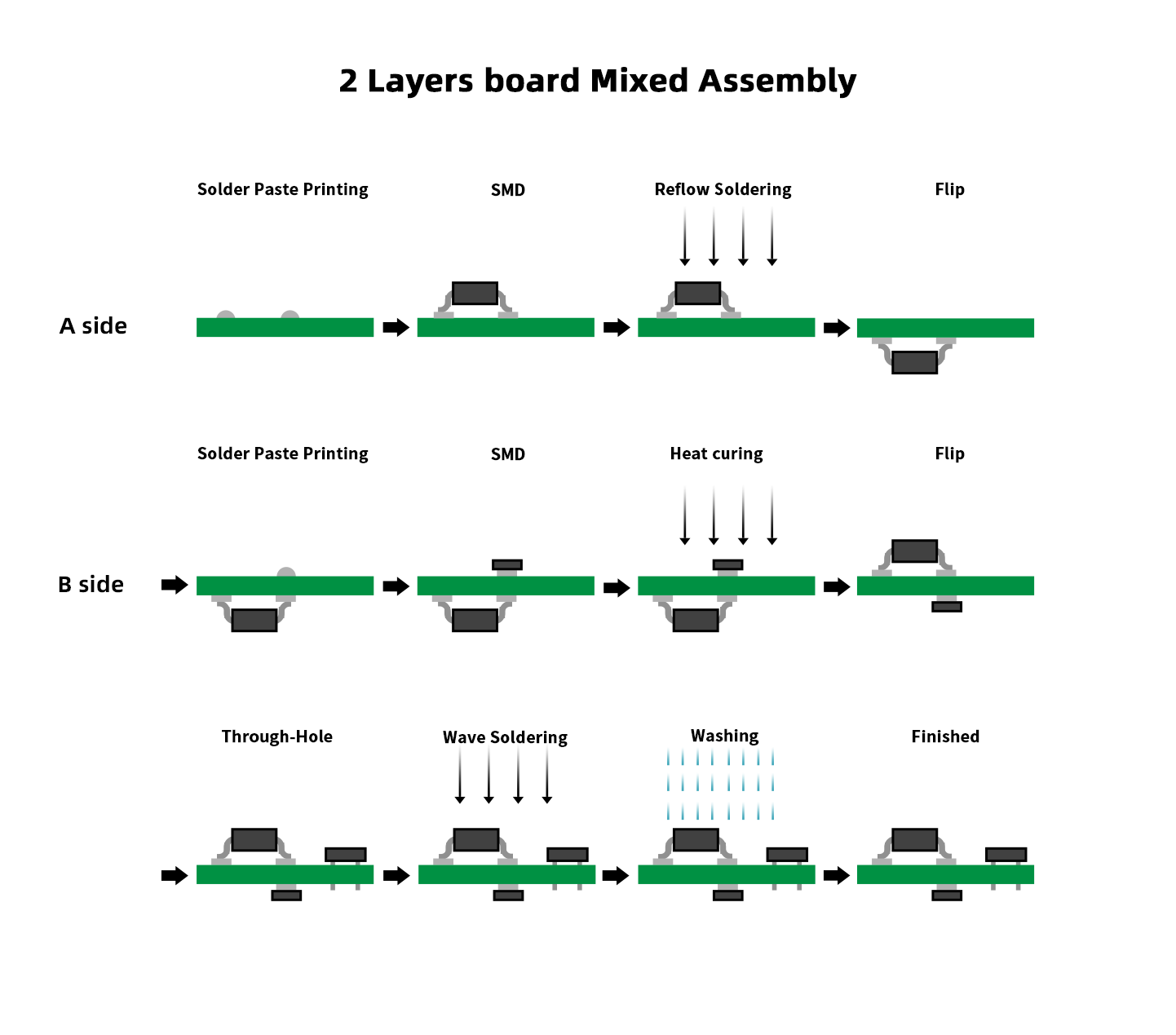
Surface mount assembly refers to the stage of the PCB assembly process where surface mount components are soldered in place. This typically occurs before through-hole assembly in mixed assembly boards.
It uses solder in paste form so it can be deposited in controlled amounts on the pads. The components are placed on top and the entire assembly goes through a reflow oven which melts the paste, joining the component leads to the pads.
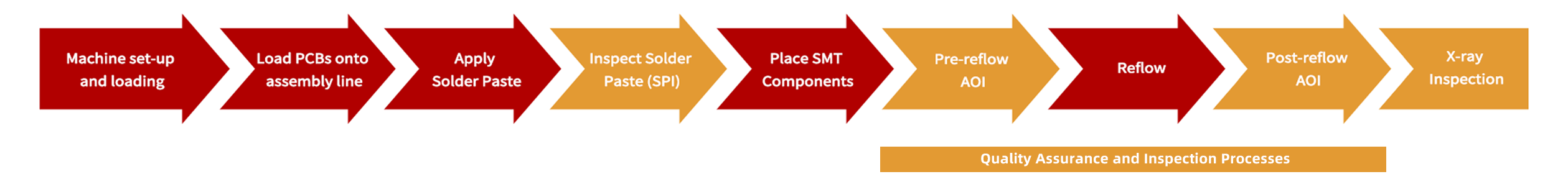
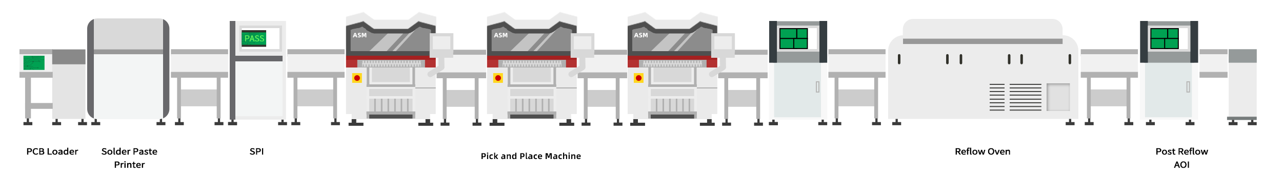
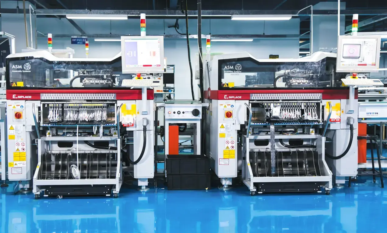
For automated assembly, the PCB boards are passed through a line of specialized machines in sequence to complete the soldering process. Here we will look at the procedure and the machines involved for double-sided surface mount boards.
The automated PCB assembly process starts with feeding the bare boards onto the line. A PCB loading machine automatically feeds them one-by-one into the solder paste applicator. Bare PCBs can be stacked up, but PCBs that already have components soldered on one side require installation on a specialized rack that leaves space between boards.
A solder paste applicator or printer, does not actually print solder paste, rather it uses a squeegee to drag solder paste over a stainless steel stencil. Solder paste consists of tiny solder alloys suspended in a liquid flux. The stencil has laser-cut holes or apertures corresponding to the surface mount pads on the PCB which allow solder paste to be deposited only where required. The thickness of the stencil determines the height of the deposited paste.
Solder Paste Printing Machine
The PCBs enter the machine and are positioned under the stationary stencil. An optical camera then locates the PCB fiducials on the PCB to check the alignment and position. Then, the boards are pushed upwards against the bottom of the stencil, and the squeegee drags solder paste over the stencil in a controlled manner.
The quality of the deposited solder paste is crucial to the quality of the solder joints further on, and most reflow solder defects can be narrowed down to issues with the solder paste printing process. Therefore a solder paste inspection (SPI) machine is invaluable in maintaining consistent quality across a batch, especially when changing solder paste or setting up a new design.
SPI machines use automated optical inspection (AOI) techniques and algorithms to inspect solder paste deposits for defects. A high-resolution camera takes images on various positions on the board which are used to compare aspects such as volume, shape and alignment against acceptance criteria. The machine flags boards that do not pass for further inspection by a technician, who will verify the defect and determine whether a reprint is required or if the solder printing parameters require modification.
SPI comes in 2D and 3D forms. 2D systems take a flat image of the boards from the top down whereas 3D systems can model structures in detail and offer much more robust analysis.
Boards that pass SPI travel to pick and place machines where surface mount components are removed from their bulk packaging and placed on their respective positions at high speed. Pick and place machines support components in multiple bulk formats such as reel, tape, tube or tray form.
Components in tape or reel form are installed in detachable feeders that facilitate the presentation of components. This includes removing the film, advancing the tape at a consistent rate and detecting jams and empty tapes. Tubes are installed at a slight angle and a vibrator ensures they travel towards the machine. Components in tray form are installed inside the machine directly within easy access of the head.
Pick and place machines have one or more pick heads on a gantry system that move suction heads or grippers with high speed and precision. A single head may have multiple suction nozzles on a rotary system, allowing it to carry and place multiple parts simultaneously, increasing efficiency.
Here is an example of how a pick and place machine would operate:
1. A camera locates the fiducial marks on the PCB panel to verify alignment and orientation is correct
2. The header moves to component inlets and picks up parts, one per nozzle/gripper.
3. The header then moves to a viewing area equipped with a camera where high-resolution images are taken to verify the orientation and check component markings. Problematic parts are set aside.
4. The head then places the part on the board according to coordinate and rotation data.
Once all the parts have been placed, they exit the machine and proceed to further optical inspection.
Often, a combination of different pick and place machines are lined-up in series for designs with a greater mix of components. Different machines are tailored to different types of components. For example, a precision machine could be required to handle 0201 and 01005 size parts or fine-pitch BGA parts. Large connectors and modules require a larger nozzle or a machine that can accommodate wider feeders or tubes.
A high-mix pick and place machine can support as many as 60+ feeders at a time. For designs with more components, loading a second machine removes the need to stop production halfway to load the remaining components. For double-sided designs, the components for the second side can be prepared while the first side is being populated, reducing downtime.
Automated Optical Inspection (AOI) performed before reflow soldering serves to confirm the placement of parts. Imaging systems can check for missing parts, incorrect orientation or alignment, etc. Most defects detected at this stage can be easily fixed by a technician and a pair of tweezers, so catching these errors before the soldering process removes the need for extensive rework afterward.
Compared to post-reflow AOI and SPI, pre-reflow AOI is used less often as it depends on the design and mix of components. For simple designs and low batches, the defect rate stemming from the pick and place process may not be significant enough to justify training the AOI machine.
After passing automatic optical inspection, the boards are ready for reflow soldering.
Reflow soldering is performed by sending the PCB boards with solder paste and components into a long convection oven or reflow oven. The process facilitates the melting of solder paste in a controlled manner to produce strong, defect-free electrical and mechanical connections.
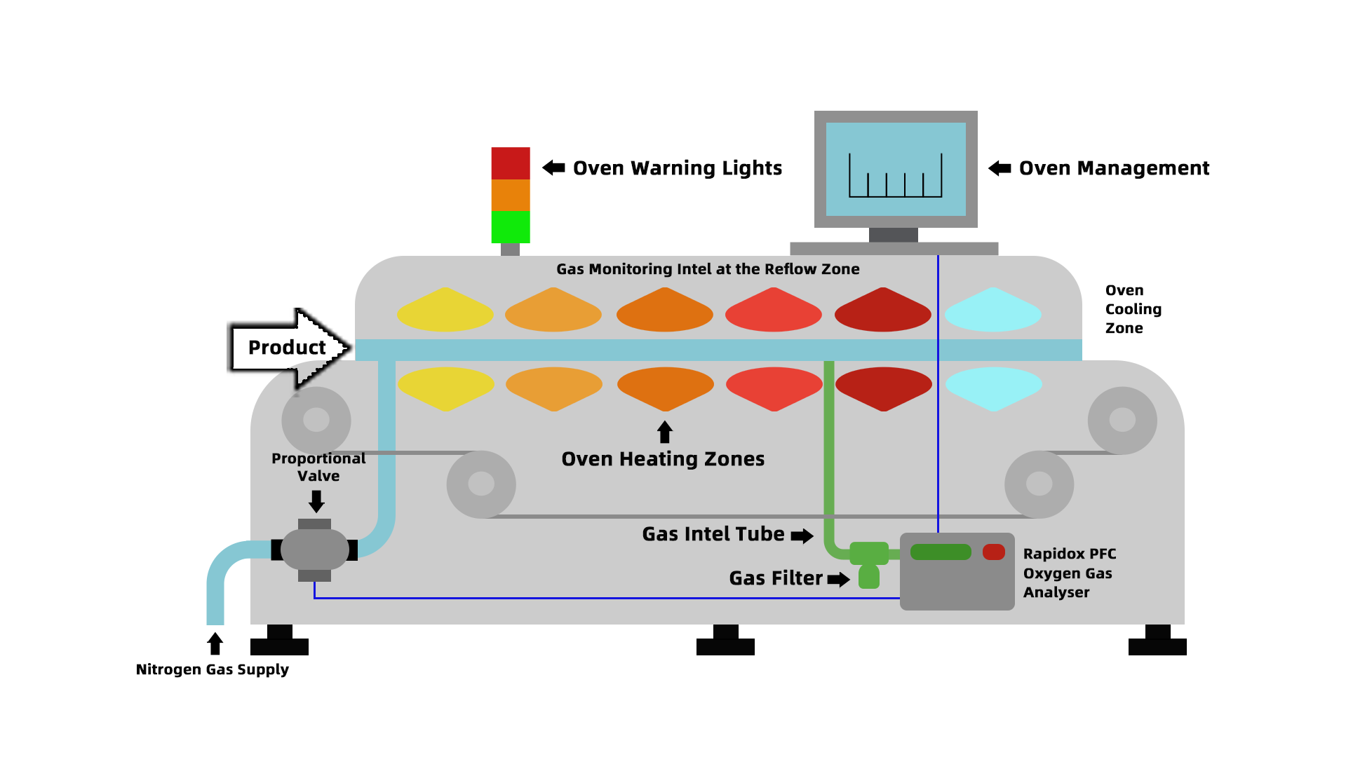
The reflow oven consists of various temperature-controlled zones regulated by a system of convection and infrared heating elements and fans. These are controlled according to a user-defined temperature profile tailored to the mix of components on the board, the board thickness, solder paste composition, etc.
The reflow temperature profile can be divided into four major phases: preheat, soak, reflow and cooling.
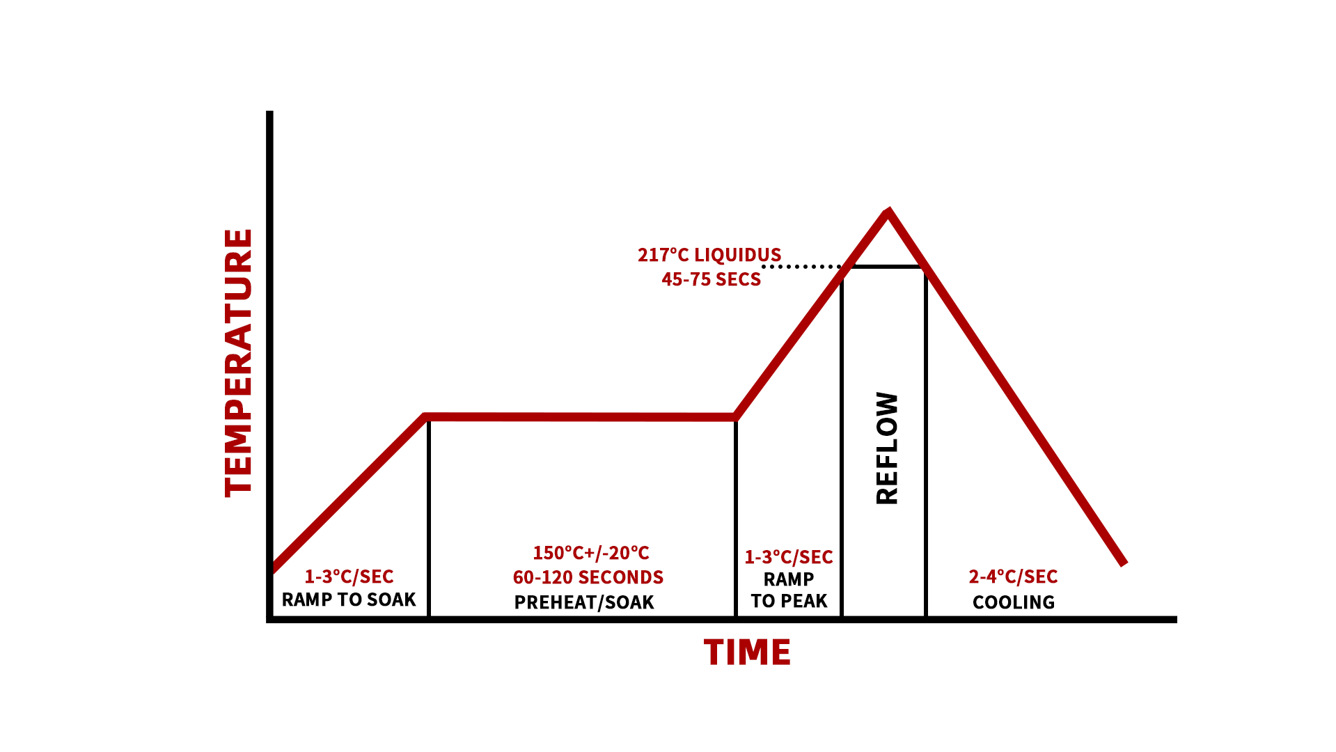
Preheat: The preheating or ramp stage serves to raise the temperature of the boards to the soak temperature in a gradual manner to minimize thermally induced stresses. As they near the soak temperature, flux in the solder paste begins to activate and expel volatile organic compounds (VOC).
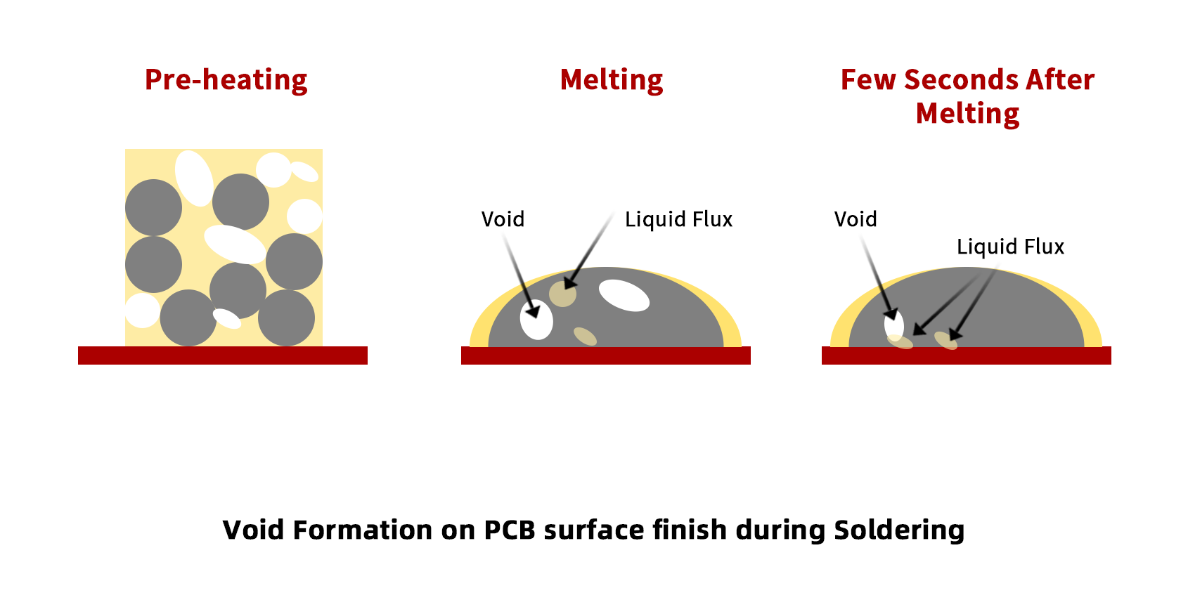
Soak: If these compounds are not fully removed from the paste, the rapid expulsion of gas at higher temperatures could cause violent explosions, resulting in more solder balls and void defects. The soak phase in the reflow temperature profile allows outgassing to occur steadily and in a controlled manner.
Reflow: The reflow stage marks where the melting of solder paste occurs. The vast majority of solder pastes are based on eutectic solder alloys, meaning they melt over a range of temperatures rather than a single point. The liquidus temperature is the temperature where melting begins which is typically 30-50°C below the true melting point of the alloy, where 100% melting occurs. By taking advantage of this, the pastes liquefy without actually reaching the true melting point.
At the reflow stage, the liquid solder flows and wets metallic surfaces, connecting the pads and component terminals.
Cooling: In the cooling phase the temperature of the boards is gradually reduced. This step is equally as important and must not be rushed to prevent thermal shock.
The temperature and time at each phase are crucial to reducing defects and producing optimal joints.
AOI performed after reflow is more common and the main purpose is to automate the inspection of solder joints visible from the outside. AOI offers a rigorous visual inspection method that is more consistent and efficient. Contrast this to manual inspections performed by a human technician who is subject to fatigue and human error and whose effectiveness is dependent on their skill level.
Defects such as solder bridges, cold solder joints, excessive or insufficient solder, cracks, tombstoning, solder balls or missing solder joints can all be reduced drastically using automatic optical inspection, with defect detection rates upwards of 90% being commonplace for advanced systems. An assembly line with post-reflow-only AOI can also cover component irregularities such as incorrect parts or orientation.
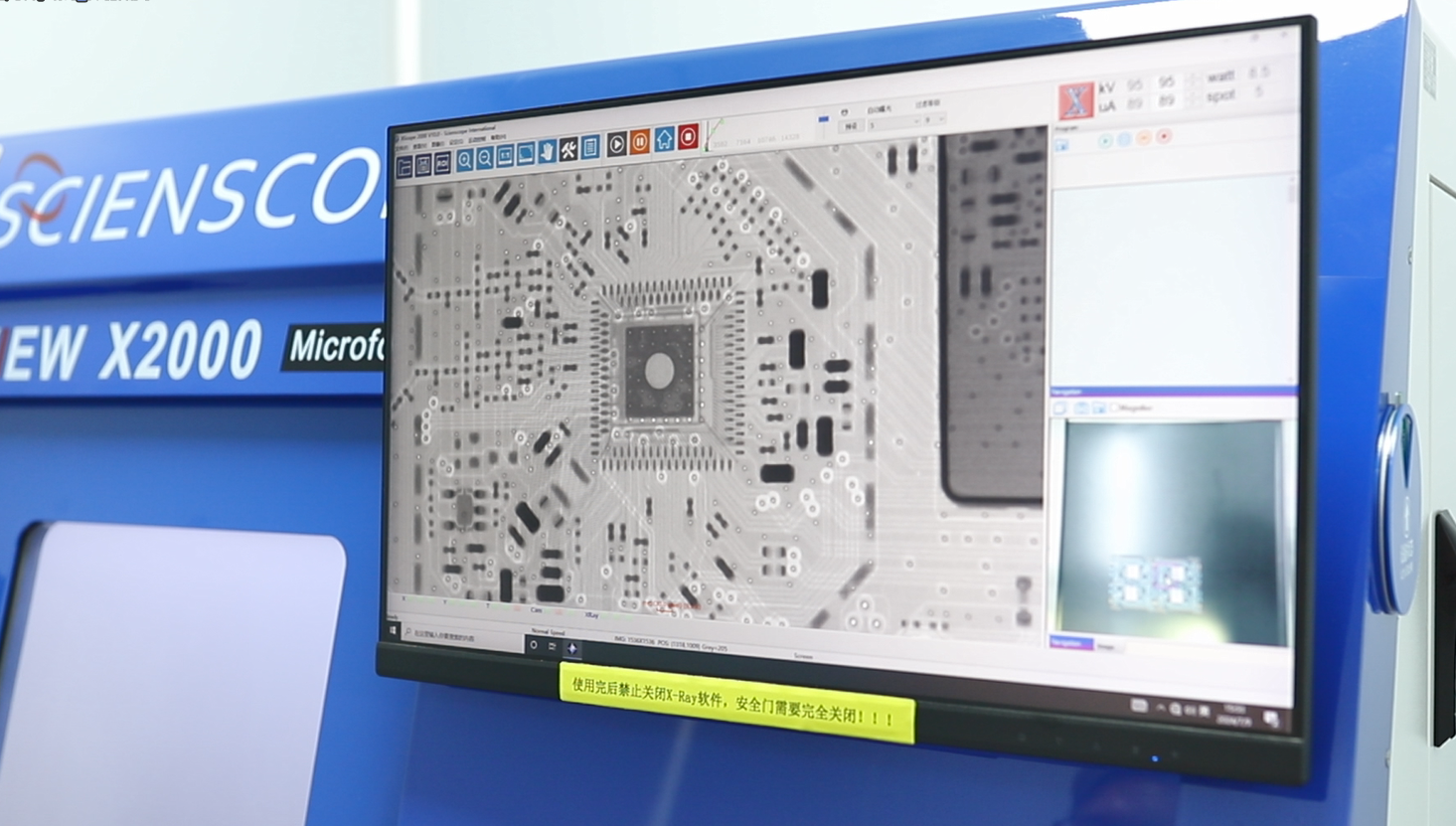
X-ray inspection is used in the PCB assembly process to inspect joints and surfaces not visible from the outside. It is commonly used for bottom-terminated components such as BGA, QFN and MLF packages or densely populated designs and can also reveal subsurface cracks, voids, delamination, etc.
The use of x-rays offer deep penetration without affecting the hardware. The boards are placed in a sealed x-ray chamber and technicians can view the x-ray images from a monitor outside. X-ray is often performed offline in non-mass production settings, i.e. they are removed from the production line, on a random sample or on samples removed periodically over a production run. This gives process engineers feedback on the production processes and may indicate if fine-tuning is required.
This completes the process of SMT assembly for single-sided boards. For double-sided SMT designs, the boards are flipped over and the same stencil, pick and place and reflow process is repeated.
Components on the first side will undergo reflow again therefore care has to be taken to ensure heavier components do not detach. This can be avoided by using custom-built fixtures that shield the components and hold them in place, or by applying special glue under the bodies of heavier components before the placement step.
For mixed assembly, soldering of through-hole components follows reflow soldering.
Through-hole assembly describes the process of filling plated through-holes that have the leads of through-hole components inserted with solder, thus binding the part electrically and mechanically to the circuit board with a strong solid solder joint through the PCB board.
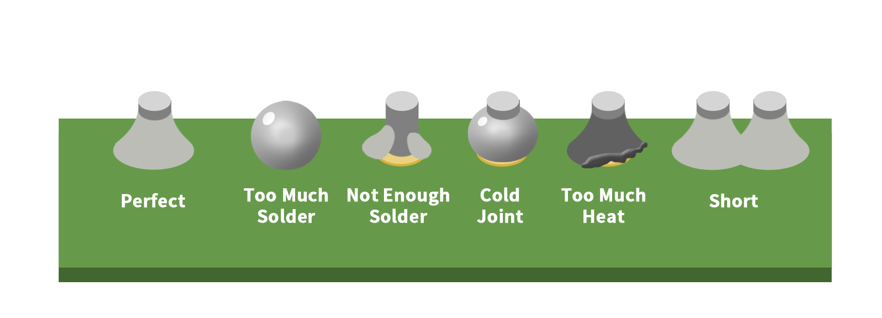
Through hole soldering defects
Many assembly houses follow IPC-Class 2 soldering quality standards. This gives a series of guidelines for inspectors to gauge the quality of their workmanship. For example, IPC states that the through-hole barrel must be filled 50% with solder to qualify as class 2. For Class 3, this value is increased to 75%.
The ideal solder joint has a shiny or satin finish with sufficient wetting angle and is free of voids, fractures, bridging, nonwetting and cold solder phenomena.
There are three main soldering methods for through-hole components: Wave soldering, selective wave soldering and hand soldering.
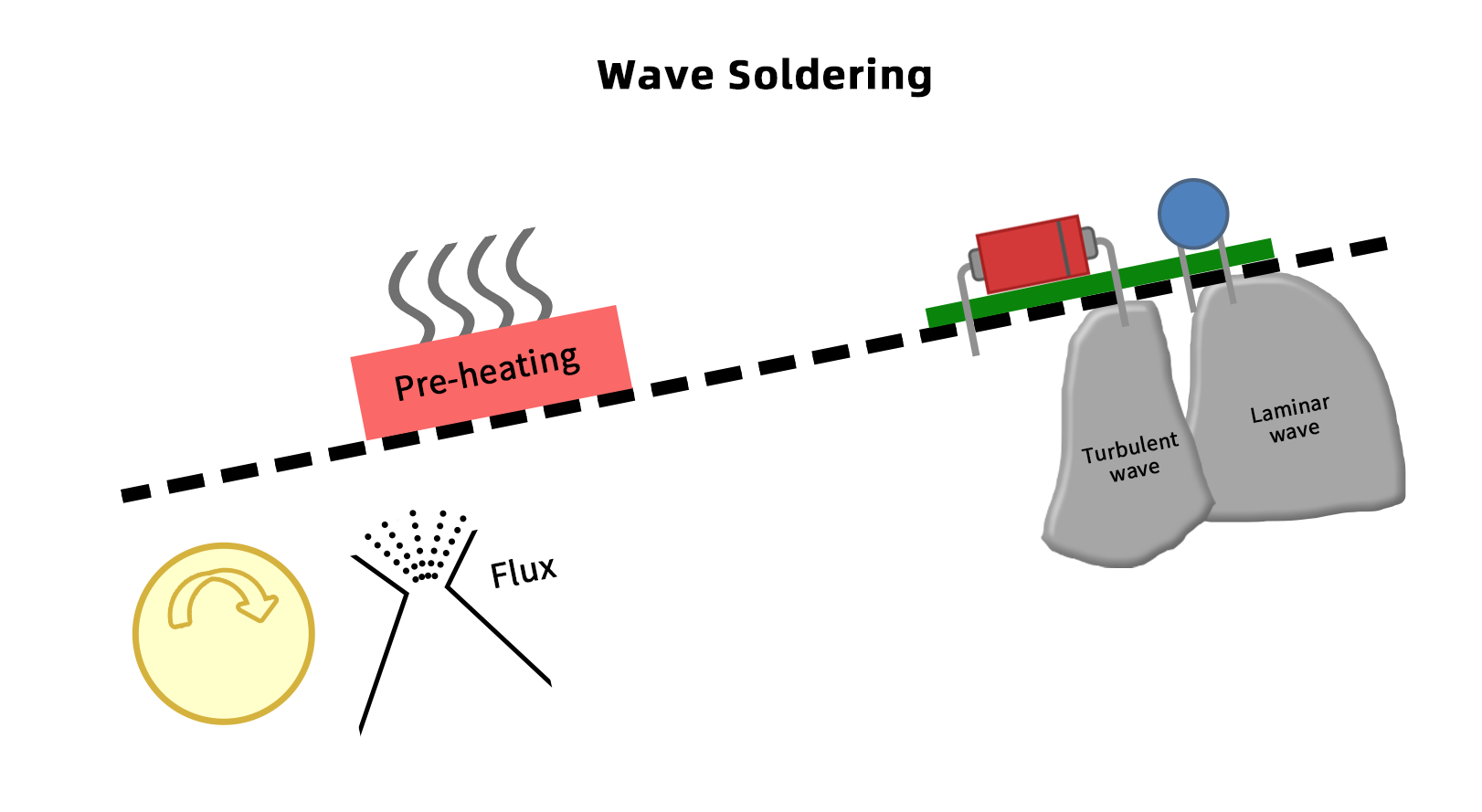
Wave Soldering
Wave soldering is an automated through-hole assembly process performed by a wave soldering machine that passes PCB boards and components over a continuous wave of molten solder to form the solder joints. This method is ideal for low density boards with a high number of through-hole components and can even be used to solder larger surface mount components in one pass.
However, wave soldering has many limitations and drawbacks, and PCB designers have to be more careful with the placement of components compared to boards intended for reflow soldering.
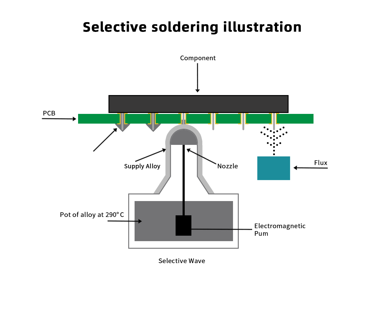
Selective Wave Soldering
For designs where through-hole assembly is not suitable, selective soldering can be used. Also known as a hybrid soldering method, selective soldering uses a system to pump a small amount of liquid solder up through a small nozzle to create a miniature solder wave. The PCB boards are installed on an X-Y table that moves the boards over the nozzle according to a preset program, thereby avoiding sensitive areas and only applying solder where needed.
This method is suited for mixed assembly designs with only a handful of through-hole joints. While selective soldering is slower, a much smaller amount of molten solder is required compared to the bath of solder in a wave soldering machine.
Manual Soldering
The previous two automated methods require a significant amount of preparation, maintenance and programming, making them unsuitable for smaller consignments. In such cases, a skilled technician with a soldering iron may be a more feasible and quicker option.
Depending on the design, a combination of the three methods may be utilized. In the following section, we describe how they may be implemented in a single through-hole assembly line. Typical designs usually only call for one or two methods.
The illustration below shows the automated wave soldering through-hole assembly process, including AOI. Here, we will look in detail at the procedure for wave soldering double-sided mixed assembly boards where the surface mount components have already been reflow soldered. This is followed by selective wave soldering of through-hole parts on the opposite side.
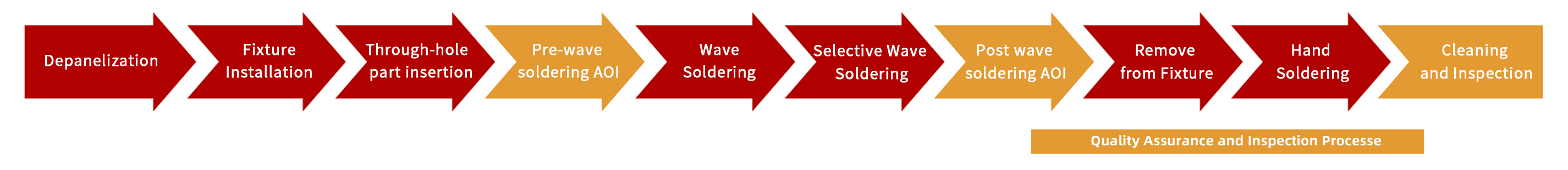
At this stage, the boards are populated with surface-mounted parts and are in panel form. For automated through-hole assembly, especially with double-sided, mixed assembly designs, the boards may require custom-made fixtures. These fixtures have openings that expose the through-hole leads and shield other components from the solder wave.
Technicians remove the individual boards by using a v-cut depaneling machine or a depaneling router machine depending on the design. They are then clamped into the fixture and placed on the assembly conveyor belt. By using a fixture, the boards can be spaced further apart to reduce disruption to the solder wave. Blocking the flow of the solder wave could prevent the solder from reaching tight areas, resulting in insufficient filling.
The next stage is to insert the through-hole components into their respective plated through holes. This can be done with automated insertion machines for large quantities or manually. When done manually, technicians sit along the assembly line and each technician is responsible for inserting one or two parts. This reduces room for error.
As with reflow soldering, the job of the first AOI inspection machine is to verify the placement of the parts. Using optical means, the AOI machine can identify missing or extra parts, incorrect orientation or crooked parts. For simple designs and small batches, human technicians may replace the AOI machine.
The boards then travel into the wave soldering machine where they undergo a preheating stage and are sprayed with a layer of flux. The preheating prevents thermal shock to the assembly and activates the flux. Flux helps the solder adhere to the pads and component leads by removing oxidation. The boards then travel slowly across the surface of a continuous flow of molten solder. Solder is pulled into the barrel of the plated holes via capillary action which solidifies as it leaves the wave and cools.
As with reflow assembly, post-assembly AOI checks the quality of the solder joints by comparing photos with trained images. Any detected failures require manual review and defective units are set aside for further analysis or repair. This completes the wave soldering process.
The boards are then removed from the wave soldering fixture and may be installed into another fixture revealing the leads of the components that could not be wave soldered. These are inserted and the assembly passes through the selective wave soldering station.
The boards again undergo a flux and preheat stage, then the selective wave soldering station follows a pre-configured program to either move the assembly above a stationary solder fountain or move the nozzle relative to the assembly. The small size of the nozzle allows it to avoid sensitive areas and target specific locations.
Finally, if there are components that cannot be soldered by wave or selective wave soldering means, the last resort is hand-soldering by a trained technician. This includes parts like wires and non-washable components that would otherwise require specific machines tailored to solder the component or require soldering after the flux residues are cleaned off the boards.
Many soldering processes involve the burning of solder flux which can leave unsightly and corrosive residues on solder joints and components. Even no-clean fluxes leave behind some chemical residue which may become conductive over time. The thin film of residue may also interfere with testing, as the film prevents the pins from making sufficient electrical contact. It is also required to clean flux residues before applying conformal coating to assist with adhesion. Therefore, most assemblies will require cleaning and this is now standard practice in many assembly houses.
PCBA Cleaning Methods
After being proven by NASA scientists, cleaning with ultrasonic baths has gone out of favor due to the harsh nature of the cleaning. Ultrasonic cleaning uses the implosion or cavitation of tiny bubbles to clean in the tightest of spaces quickly and efficiently, but the action also causes damage to a wide variety of components and structures.
Other cleaning methods include manual cleaning with flux cleaner solution or with high-powered dry ice cleaning stations depending on the chemistry of the flux used. The dry ice blasting method fires pellets of solid CO2 at high velocity. As they make contact with the surface they undergo sublimation where they convert directly from a solid to a gas. This action lifts contaminants off the surface without the need for water or solvents. The low impact also minimizes damage to components and joints.
This completes the soldering process from surface mount to through-hole assembly. The completed boards undergo another final inspection before being packaged and shipped to the client. However, there are other services offered by contract manufacturers designed to reduce defects, provide extra protection and help finish a product.
PCB assembly factories utilize a variety of inspection and testing strategies to maximize yield and ensure the quality of their client’s products as best they can. In addition to standard inspection practices, advanced manufacturers go above and beyond and work with clients to offer additional testing services. Here are some strategies assembly houses employ to reduce the number of defective units reaching clients.
Through-out every step of the manufacturing process, visual inspections are carried out periodically to monitor ongoing manufacturing processes. As shown in the assembly line diagram, each machine is separated by an inspection station where an operator can examine or intercept sub-standard assemblies. This is especially important for small batches, as the processes are not as fine-tuned as in mass-production settings and may need to be tweaked as they are being produced.
In-circuit testing or ICT of a PCB assembly tests the electrical behavior of the device under test (DUT) to find faults. Unlike ICT of bare PCBs, PCBA ICT is more involved and a variety of test instruments and strategies are required to fully test a device.
Bed-of-nails testing
Batch PCB assemblies can be tested using a custom-made test jig or bench, otherwise known as a bed of nails fixture which offers a quick way of testing multiple points on a device. The test jig has spring-loaded pins for every test node on the PCBA which make contact when pressed down. The program then transmits a series of electrical signals and records the response to validate the device.
Flying Probe testing
For bare PCBs, flying probe testing is used extensively for a high mix of PCB designs where it would not be feasible to build test benches for each design. For PCBA, flying probe testing is also available however, it is not as flexible as PCB FPT.
Set-up takes much more preparation and requires calibration with a test board, making it unsuitable for small prototype orders.
The test time per piece is longer as only a few probes are available to test all nodes as opposed to testing of all nodes simultaneously with a bed of nails.
The advantage of 3D flying probe testers is their flexibility. Software-controlled 3D rotation allows them to reach more concealed areas and use component leads as test points.
ICT testing can effectively detect opens and shorts, component placement errors and defective parts, however, this alone does not ensure the device functions correctly. For this, functional testing is used.
Functional testing, as the name suggests, tests the functionality of the PCB electronics according to the client’s specifications. Unlike ICT, functional testing is a black-box testing method that only evaluates the behavioral outputs without knowledge of the internal design. This is simpler for contract manufacturers to take on, as it only requires the client to instruct them how to perform the tests and what behaviors to look out for.
Many turnkey PCB assembly houses welcome and even encourage functional testing as it helps to verify the entire turnkey process - something not possible with other test methods. Based on the results, manufacturers can work with the client to investigate the cause and make improvements to production processes before or during production.
However, functional testing may have trouble verifying the quality of electrical signals and highlighting underlying faults. Depending on the level of coverage, functional testing can be labor-intensive and difficult to scale up.
Programmable devices such as microcontrollers, CPLDs and FPGAs are often purchased without firmware. Programming instructions have to be loaded onto the devices before the product can function, therefore assembly houses that offer functional testing services also support firmware burning.
There are generally two ways a manufacturer can help load firmware onto PCB assemblies:
Manual Burning after assembly
Firmware can be burned onto the devices after soldering processes by using designated ports or pads designed on the circuit board which connect to the target pins of the microcontrollers. Technicians connect the burner device and run the programming software which writes the firmware.
This approach requires a designated interface to break out the target pins on the MCU which may not be desirable for compact designs. The process can also be labor intensive or require custom jigs to simplify operation. If a device has a test jig and functional testing procedure, the firmware burning process can be included with the test process if it does not incur significant additional labor or test time.
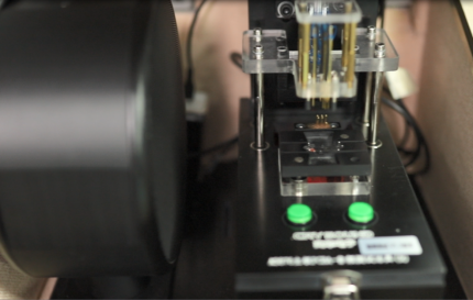
IC Programming before assembly
Alternatively, chips can be programmed before assembly using a special fixture or a IC programming machine. An IC programming machine picks up chips in tape, tube or tray format and places them into the burner unit. The unit can burn multiple chips simultaneously without assistance. It then places the programmed chips back into the tray or seals them in a new reel ready for assembly. A colored indicator can also be marked on the chips to indicate that they have been pre-programmed and distinguish them from non-programmed chips.
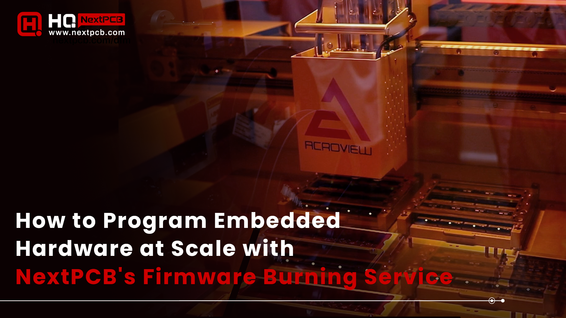
An IC programming machine saves on labor costs and speeds up production for large batches, as the chips can be burned automatically before production. This particular machine can program up to 32 chips at one time and supports various chip types in various packages including MCUs, FPGAs, CPLDs, NOR/NAND Flash, eMMC and Universal Flash storage devices.
Leading EMS companies often have the capability to provide product certification services or assist with testing required to comply. This includes safety certifications like UL, CSA and TUV; EMC/EMI compliance for CE and FCC; environmental certifications such as RoHS and REACH; wireless certifications and automotive, medical and industrial control standards.
Dedicated product certification experts will be able to assist you in achieving your product certification goals without the need for in-house testing facilities.
Many EMS providers also offer services that bring a PCB Assembly closer to the finished product. This may include electromechanical assembly, box assembly and kitting.
Electromechanical Assembly
Integrating PCBAs with mechanical components (cables, enclosures) for finished products: Electromechanical assembly describes the process of combining electrical and mechanical components to the whole assembly such as connecting cables and wires harnesses, installing mechanical parts and mounting into the enclosure. This requires specialized equipment and training for building mechanical assemblies. Some contract manufacturers will also have their own preferred suppliers for wiring and manufacture of mechanical parts, further alleviating the client’s workload.
Box Assembly and Kitting Services
Box assembly and kitting refers to the process of packaging the product and procuring accessories such as labels, instruction manuals and cables that are delivered with the product to the customer. This is ideal for finished products that will be sent directly from the factory to the customer or distributors.
Conformal coating or potting services are additional services designed to provide additional protection to electronic assemblies against environmental contaminants and moisture and are ideal for devices designed to endure harsh environments such as in marine, agricultural and industrial settings or for waterproofing consumer electronics.
Conformal coating is a thin film applied on the surface of the PCB assembly either in spray, gel or liquid forms that solidify when cured. Common solutions used include acrylic, urethane and silicone-based mixtures.
With potting, the PCBA is installed into a closed potting enclosure and the potting solution is poured into the cavity, filling all gaps and providing more protection than conformal coating.
Solutions with high thermal conductivity and elasticity are available to assist with heat dissipation and prevent cracking with thermal expansion.
Some products require unique or custom identification codes printed on their PCB assemblies such as QR codes printed on smart home products. This can be performed using a laser engraving machine before the bare PCB boards are populated. Different laser types can be used to mark different surfaces such as the bare PCB substrate, solder mask, silkscreen and even aluminum stiffeners on flexible PCBs.
Laser marking is also used to track PCB assemblies during the manufacturing process. Operators can scan the codes and look up the details in the Manufacturing Execution System (MES).
As we have already seen, many factors go into determining the complexity and therefore the cost of producing an electronics product. Many factors are determined by the PCB’s design and the choice of components which is intrinsically linked to the assembly type. These are factors within the designer’s control.
A common misconception by first-time designers is that they get to pick and choose which production methods are used to produce their designs. This is rarely the case. The methods used are dictated by the specific design, the production volume and the capability of the assembly house. Therefore, identifying the desired production method before beginning a design can ensure the design is appropriate.
Manual methods are often frowned upon for having inferior quality workmanship compared to machine assembly, and clients may request that all parts be machine assembled. It is not impossible, however, there are a number of reasons why few assembly houses will entertain the idea of setting up an entire assembly line to solder 2 or 3 prototype boards:
Manual assembly is not necessarily bad. Defective boards from automated assembly lines are often sent for rework which requires the dexterity and judgment of a skilled technician. Without a trained eye, most would not be able to tell the difference between solder joints made by automated equipment compared to by hand.
The interpretation of manual soldering is also at fault here. Hand soldering does not equate to a technician soldering surface mount chips with a soldering iron and a piece of solder wire. Various rework techniques and a combination of semi-automated strategies can make the best of both worlds without compromising quality or efficiency.
It is important to understand the equipment available to your assembly house and their standard practices. A combination of manual and automated means and a little care and attention is more than enough to produce PCB assemblies on par with mass-produced specimens. Even small batch runs of several thousand pieces may not justify automating through-hole insertion or soldering. There are also limitations imposed by specific components and design decisions that may hinder automated assembly.
Small batch assembly houses have access to machine assembly equipment and may perform the solder paste printing and pick and place steps manually, then send them through the reflow oven. The pick and place step may also be automated to take advantage of the additional precision, especially for small parts such as 01005 and 0201 size chips and fine-pitch BGAs.
The opposite is also true for large batch runs. Choosing components that have to be soldered manually will result in hefty labor fees or even complete refusal by your assembly house. They may not have the available manpower or time to manually solder thousands of parts.
For example, in prototyping and hobbyist projects, it is common practice to pull apart the three leads of a transistor to fit the triangular footprint. If this footprint and component are used for mass production, technicians would have to pull apart the leads and manually solder potentially thousands of these parts, not to mention trimming of leads. By simply switching to a bulk packaging footprint and/or part, these problems go away.
The question of how your PCB design will be assembled comes down to factory floor process engineers who base their decisions on factors including time, cost, labor and quality of automated and manual means for each step and machine. Even with all the manufacturing documentation available beforehand, it can be difficult to predict the most effective assembly strategy for complicated mixed designs.
As a designer, better decisions can be made to simplify a design to make it easier to manufacture at the best quality possible at all stages. By actively minimizing potential complications you, your assembly house and your wallet will thank you.
This could mean keeping components on one side (top or bottom only) and using surface mount parts where possible.
The choice between surface mount technology (SMT) and through-hole (THT) components significantly affects PCB manufacturing cost.
A common conundrum for beginners is whether to use surface mount or through-hole components for their design. Many design-based and manufacturing-based factors play a part in this decision but it goes without saying that the design specifications take priority ahead of the manufacturing impact.
As a general rule of thumb, unless you are hand-soldering a couple of boards yourself that won’t go to scale, surface mount parts are almost always preferred in terms of ease of manufacturing. This applies to prototypes or producing at scale with your assembly partner. Since most designs have some surface mount components, most assembly houses will assume reflow soldering will take place, regardless of the quantity. Some providers do not even offer through-hole soldering altogether or offer it in a limited capacity.
Traditionally, through-hole parts were used when product size was not a priority and electronics only penetrated the surface of the consumer market. As reduced costs made electronics more accessible and the demand for smaller, sleeker and more powerful electronics grew, the drawbacks of THT components rapidly pushed designers towards newer surface-mounted technologies.
Size:
Difficulty of assembly:
While through-hole parts have many disadvantages, THT parts are still widely desired where additional mechanical strength is required, such as large and heavy parts (e.g. power electronics) or parts that require greater durability such as user-accessible connectors that need to withstand repeated plugging/unplugging over its lifetime. They are also widely used in prototyping and breadboard projects and for teaching basic electronics and soldering skills.
In the world of manufacturing, the general rule applies that as production volume increases, the cost-per-unit decreases - a principle known as "economies of scale."
This is because larger-scale manufacturing provides access to a range of efficiencies and cost-saving opportunities that are not feasible or not available to smaller-scale operations.
Fixed set-up costs can be spread over a greater number of units, granting access to more capital-intensive but more efficient production methods and technologies. Operations can be streamlined and manufacturers can leverage greater purchasing power to negotiate not just lower material costs, but better expertise and services from suppliers.
However, it's important to note that this trend of decreasing costs per unit does not continue indefinitely. There is typically a limit or "optimal" production volume beyond which the advantages of scale may start to diminish. Factors such as supply chain complexity, coordination challenges, and overhead burdens can offset the benefits of further increasing scale.
By understanding the manufacturing challenges and eliminating operations that scale up poorly, designers can significantly reduce mass production costs and complexity.
On the other hand, fixed costs can have a big impact on repeated small runs as with the case for prototyping and small batches.
Costs may be equally affected by fixed and non-fixed costs. Striking a good balance is key to achieving the best cost efficiency.
Take the Bill of Materials for example. Turnkey manufacturers have to source and perform quality control for each different part (or BOM line). During assembly, each different component has to be prepared, installed into a feeder/receptacle and programmed. These contribute to the fixed assembly costs in cost calculations and can stack up in small batch runs.
By choosing ‘multipurpose’ parts with values that can be used in multiple positions, designers can reduce the number of unique parts, thereby reducing component fixed costs.
Choosing the right PCB assembly partner for you depends on a variety of factors. First ask yourself your project needs, forecast, budget and any additional services you will need and how involved do you or your business intend to get involved with the manufacturing process.
Assembly houses may use words such as prototype, small batch/high mix or mass production to describe their services. This can generally tell you whether you and a manufacturer are a match from the offset.
Manufacturers that focus on prototype orders have services catered to small volumes of a high variety, or high mix. They typically have the capabilities to tackle high-difficulty designs and the flexibility to accommodate custom requests. Much of the assembly process is done manually on an order-by-order basis.
Small batch PCB assembly services (100-5,000 units) cater to high-value industries like medical and aerospace. High-mix refers to either the mix of products that they process or the mix of component types on the boards. Also known as agile manufacturing services, they can deal with custom requests and mid-production changes that would severely disrupt larger volume manufacturers by emphasizing flexibility.
Small-batch high-mix services are suitable for small production runs of high-value goods where failures are not an option, such as in medical, aerospace and industrial applications. Volumes are small enough to be able to test all devices, repair defective units and perform custom operations manually.
Volume PCB manufacturing facilities specialize in large-scale consumer electronics. The factory giants of hardware manufacture, these are the Foxconns and producers of everyday consumer electronics. Highly specialized systems, the assembly lines are designed to produce a handful of products of a few variants with minimal changes. Due to the sheer volumes produced, production engineers invest a significant amount of resources to reduce the defect rate but not eliminate failures entirely. They often also perform the final box build and electromechanical assembly for the product.
There is no hard and fast rule as to how many devices or components qualify as prototype, small batch and mass production volumes and there is substantial overlap between the categories. Batches of several hundred pieces may be used for prototyping a mass-produced product, and several thousand pieces may be easily handled by a small batch manufacturer, depending on their structure and capabilities. Some small batch providers may also accept requests for a handful of pieces.
Turnkey PCBA encapsulates parts procurement and PCB manufacture in addition to PCB assembly, as opposed to consignment which only includes PCB assembly. The decision between choosing turnkey or consignment falls upon your organization’s supply chain and procurement capabilities, and how they compare to that of turnkey PCBA providers.
Whether for electronics components or PCBs, adept contract manufacturers have robust supply chains and dedicated purchasing agents that work with an established network of distributors and original manufacturers. While major distributors have vast, up-to-date online catalogs, finding all the parts needed for your design can still be a challenge, especially at the required price point. Capable purchasers can find hard-to-source parts and alternatives at lower costs.
With a greater volume and mix of orders, contract manufacturers have greater purchasing power for a wide variety of materials. They can also better negotiate agreements and processes in the event of supply chain issues, allowing them to better control quality and ensure authenticity. A good turnkey provider will also check incoming components and PCBs for quality and correctness and handle any disputes.
This offers various advantages for product developers, allowing them to focus on developing new designs:
On the other hand, consignment is advantageous if your organization already has the resources to procure materials for your needs and you need greater control of materials. For most startups and SMEs, turnkey PCB manufacturing reduces risk and operational overhead.
The decision between choosing to go turnkey or consignment is closely tied with the decision to go with local or overseas assembly providers. With local service providers, since the supply chain is based locally, the advantages of turnkey manufacture are not as profound.
With overseas manufacturers, turnkey formats make much more sense since the manufacturer’s supply chain is also based overseas. This allows customers to diversify their supply chain and penetrate into supply chains that better suit their needs via a turnkey service supplier. This is especially important if there are language and payment barriers, such as with suppliers in Asia. The turnkey provider can communicate and navigate the supply chain on the customer’s behalf and find low-cost alternatives to big brands and handle logistics and customs clearance on your behalf.
In this discussion, local or domestic operations refer to a supplier in the same country or continent as the destination country in Western countries, compared to cheaper manufacturing providers in the East and South.
Cost is the primary reason for contracting to overseas PCB assembly providers and taking advantage of the supply chain benefits. Those who can afford to stay local have the advantage of being able to market the product as being made locally and thus command a higher retail price. The manufacture of certain military and IP-sensitive products can also be limited to certain regions, for example, ITAR regulations in the US control the export of defense-related articles and information.
Cost-sensitive products can take advantage of the lower labor, overhead and operational costs of overseas operations such as in Mexico, India and China. Cheaper, however, does not necessarily mean lower in quality. Manufacturing hubs have the advantage of experience, high order volume and heavy investment in new technologies that allow for greater efficiencies, more capabilities and higher product quality.
|
|
Local |
Overseas |
|
Cost |
|
|
|
Supply Chain |
|
|
|
Communication |
|
|
|
Lead Time |
|
|
|
Capabilities |
|
|
Table highlighting the differences between local and overseas PCB assembly houses
The word broker tends to illicit negative connotations, and it is not uncommon for them to disguise themselves otherwise. However, brokers can be the best match for organizations or individuals that can benefit from their additional care. Brokers often have the freedom to focus on offering other support services or optimizing their services to specific markets.
On the other hand, purchasing directly from the manufacturer has many advantages in addition to lower costs and faster turnaround. Clients can benefit from direct access to engineering expertise which allows for faster issue resolution and personalized guidance. Factories are also more likely to take in and act upon customer feedback to improve processes and services.
Manufacturer capabilities and quality certifications can vary greatly across the industry. Preferably before beginning the PCB design, evaluate your product’s specification and key components and generate a checklist of special features and services required and at what volume. Then assess the manufacturer’s technical capabilities, equipment and certifications to ensure they can produce your product to spec. Once these are determined, evaluate samples for quality and workmanship.
The turnkey provider’s PCB manufacturing capabilities can be as important as their assembly capabilities. If they do not have the capabilities to produce your PCB boards then you may need to find a manufacturer yourself and have them sent to the assembly house, losing out on a major convenience of turnkey services.
When selecting a PCBA (Printed Circuit Board Assembly) partner, it is crucial to inquire about the types of assembly they are capable of handling and any other specialty services required. This information can help you determine the suitability of the assembly house for your specific project and future project requirements. Here are some example considerations:
An assembly house’s arsenal of equipment is an important metric in gauging the size of their facilities and their abilities. A small assembly house may have just one or two assembly lines that run constantly for all their orders. This severely limits flexibility and efficiency. For example, machines such as the reflow oven may be set on a universal setting, which is not optimal for non-standard, specialty designs. With just one or two assembly lines, the factory’s output reaches a bottleneck as they wait for machines to be loaded and programmed.
A factory with many assembly lines, even if they are not operational all the time, has the freedom to pick and choose the best equipment for the order and prepare them in advance. They are also more adept at dealing with a sudden influx of orders or equipment breakdowns, allowing them to plan ahead and meet customer’s deadlines more effectively.
For turnkey services, the manufacturer’s supply chain capabilities could be just as important as their manufacturing capabilities. You will want to leverage their purchasing power, infrastructure, supply network and quality relationships to achieve the lowest costs with peace of mind.
Last but not least, the quality of the service and communication can make or break a partnership. In recent years, online ordering platforms have become popular, especially for overseas companies that may not share the same time zone with the customer. They allow for price transparency, which can be used to gain insight into pricing structures and compare costs across suppliers.
While convenient, they are not to everybody’s liking and can vary in user-friendliness. Some assembly providers have unfortunately become overly reliant on online platforms, abandoning the more traditional quotations by e-mail and personalized support. Having a direct point of contact or dedicated account manager with good rapport can save a lot of time and hassle, compared to bouncing between multiple customer support agents.
Differentiating between the production quality of different manufacturers can be a challenge. Online reviews can be biased and a single damming review from a disgruntled customer may be a poor reflection of their overall services.
To gain a more comprehensive understanding of a manufacturer's emphasis on quality, it is crucial to evaluate a broader range of factors. Some key elements to consider include the manufacturer’s quality systems and certificates, testimonials/endorsements and equipment.
Industries such as automotive, medical and aerospace have elevated quality standards and may demand stricter quality acceptance criteria compared to consumer electronics.
While not necessary, having the production facilities evaluated by an accredited third-party organization shows the manufacturer’s quality management capabilities and commitment to quality and other regulations. Some quality management system certifications to look out for include:
ISO 9001 - Generic QMS
ISO 14001 - Environmental management
IATF 16949 - Automotive industry QMS
ISO 13485 - Medical devices QMS
AS9100 - Aerospace and defense industries QMS
IPC-A-600 and IPC-A-610, are acceptance criteria standards for bare PCBs and electronic assemblies respectively. While not quality management systems and not certifiable, manufacturers often state compliance with the classification levels defined in these standards to give an indication of their level of workmanship.
Manufacturers that go above and beyond IPC Class 1, the most basic level, have a strong emphasis on quality.
In addition to certifications, it is valuable to look for examples of the manufacturer's prior work within the same industry as your own product. Reviewing these industry-specific products can provide valuable insights into the manufacturer's workmanship, quality standards, and ability to meet the unique requirements of your sector.
In combination with quality metrics, a manufacturer’s equipment and standard practices can paint a better picture of how they manage the quality of their products.
For turnkey PCBA, numerous techniques can be employed to reduce and identify defects during production including incoming parts inspection (IQC), first article inspection (FAI), AOI, x-ray and visual inspections and electrical and functional testing.
AOI machines are some of the most expensive machines on an assembly line and are essential to catching defects reliably in large batches. A typical SMT assembly line will have at least two AOI machines; one in the form of an SPI machine which is a form of automated optical inspection and one after reflow assembly. Assembly houses that do not employ AOI, put their customers at risk.
> Recomend reading: PCB/PCBA Test Methods by Category
NextPCB is a global leader in PCB manufacturing and turnkey assembly. As the international division of the renowned HQ (Huaqiu) Electronics group, we leverage over a decade of expertise, self-built solutions and state-of-the-art production capabilities to deliver unparalleled PCB solutions to customers around the globe.
With headquarters in the Silicon Valley of Hardware, Shenzhen and 5 factories and multiple components storage facilities located across China, HQ NextPCB is strategically positioned to deliver affordable, high-quality and efficient PCB manufacturing and assembly services.
Introducing Rev 0 — Our Brand-New PCBA Ordering Experience
We've completely reimagined the way you order PCB assembly prototypes. Rev 0 is NextPCB's newly launched ordering workflow in 2026, designed to make turnkey PCBA faster, simpler, and more transparent than ever — from uploading your files to receiving your finished boards.
>>> Try the New Rev 0 PCBA Process →
NextPCB Company Snapshot
|
PCBA Format |
Overseas Turnkey |
HQ NextPCB utilizes its expansive global supply chain to maximize the advantages of its turnkey PCB assembly services and deliver them customers around the globe. PCBs are also fabricated by NextPCB for seamless integration. |
|
Volume |
Prototype, Small and Mass Production |
From 5 pieces to hundreds of thousands, with dedicated factories for prototype, small and mass production PCB manufacture and assembly, NextPCB is ideal for scaling up products under one roof. |
|
Factory/Broker? |
Direct from Manufacturer |
As part of HQ Electronics, with NextPCB you get direct from manufacturer prices, expertise and efficiency all in-house. |
|
Support/Ordering Format |
Instant online quotation + key account managers |
Get the best of both worlds with an advanced instant online quotation platform for both PCB and PCBA, and personal key account managers for custom requests and queries. |
|
Factory Capabilities |
|
Over 36 lead-free assembly lines equipped with advanced AOI, pick and place and X-ray machines for double, mixed wave and reflow soldering ensure maximum efficiency and flexibility. PCB fabrication capabilities of up to 32 layers, HDI III blind/buried vias, IPC Class 3, with Rogers, rigid and flex substrates and more. |
|
Quality Certifications |
|
NextPCB has proven its ability to produce high-quality electronics that satisfy strict industry standards: ISO 9001 - Generic QMS ISO 14001 - Environmental management IATF 16949 - Automotive industry QMS ISO 13485 - Medical devices QMS IPC-A-600 and IPC-A-610 Class 2 as standard. Class 3 available. |
|
Engineering Services |
|
Functional Testing IC Programming FCC/CE Certification Assistance DFM and DFA |
|
Other Services |
|
Electromechanical Assembly and Kitting Conformal Coating and Potting Laser Engraving |
Pioneers in the smart electronics manufacturing industry, NextPCB is backed by over a decade of proven expertise, reaching new heights in efficiency and optimization.
At the heart of NextPCB’s manufacturing operations lie their independently developed Manufacturing Execution System (MES), tailored to monitor and streamline material management and production processes, and connect the entire process from PCB production to assembly.
Developed in-house in tandem with production engineers, the MES system provides complete transparency and improved efficiency throughout the manufacturing lifecycle, allowing them to maximize quality and reduce costs at the same time.
NextPCB also use its manufacturing expertise to develop HQDFM, the free PCB Design Analysis Software to help engineers review and improve their designs from a manufacturing perspective and avoid production pitfalls.
Visit NextPCB for more information and try the instant online quotation platform.
We know that moving from a bare board to a fully assembled product can bring up a lot of questions. Based on common discussions and pain points shared in engineering communities like Reddit's r/PrintedCircuitBoard and r/AskElectronics, here are the top questions developers ask before ordering PCB assembly.
Q: What exact files do I need to submit for a seamless PCBA order?
To avoid your order being placed on hold, ensure you provide these three critical files:
Q: Why is the setup fee for low-volume prototype assembly relatively high?
It is completely normal to wonder why assembling 5 boards can sometimes feel disproportionately expensive compared to 50 boards. The reason lies in the fixed costs required to start the assembly line:
Pro Tip: To optimize costs, consider bumping up your prototype quantity slightly to distribute the setup fee, or utilize NextPCB's economic turnkey assembly options.
Q: How can I avoid common assembly failures in my design? (DFA Basics)
Practicing Design for Assembly (DFA) is crucial to save time and money. The most common reasons for assembly delays include:
Q: Should I choose Turnkey or Consigned (Kitted) PCB Assembly?
This depends entirely on your project's supply chain requirements:
>> Explore More at NextPCB Accelerator - Supporting You from Prototype to Mass Production
The NextPCB Accelerator campaign is an innovative initiative that empowers creators to bring their ideas to life. Whether you're an entrepreneur or enthusiast, we support your journey from concept to mass production.
Discover All Sponsored Campaigns
Still, need help? Contact Us: support@nextpcb.com
Need a PCB or PCBA quote? Quote now

