
 NextPCB Capabilities
Printed Circuit Boards
NextPCB Capabilities
Printed Circuit Boards
 PCB Assembly
 Layer Buildup
 SMD-Stencils
 PCB Design-Aid & Layout
 Mechanics
 Quality
 Drills & Throughplating
 Factory & Certificate
 PCB Assembly Factory Show
Certificate
PCB Assembly Factory Show
Certificate

Support Team
Feedback:
support@nextpcb.com


Most engineers think PCB manufacturing lead time starts the moment they hit "submit." It doesn't — and that gap is why a "7-day" quote often turns into three weeks. Standard PCB manufacturing lead times range from 5 to 10 working days for multilayer boards, while a quick-turn PCB prototype can finish production in just 24 to 72 hours. However, the real PCB manufacturing time relies entirely on your specifications: a simple 2-layer design will always move faster than advanced HDI, rigid-flex, or high-reliability boards. Ultimately, your real timeline comes down to five core factors: design complexity, material selection, fabrication processes, reliability targets, and end application. This guide breaks down typical PCB manufacturing lead times, the variables that impact them, and how you can get your boards faster without compromising quality.

The exact lead time varies between PCB manufacturers and depends on the specifications of the order. The following ranges are commonly used as a practical reference.
| PCB Type | Typical Manufacturing Lead Time |
|---|---|
| Simple 1–2 layer PCB prototype | 2–5 business days |
| Standard 4-layer PCB | 3–7 business days |
| Standard multilayer PCB | 5–10 business days |
| HDI PCB | 7–15+ business days |
| Flexible PCB | 5–10+ business days |
| Rigid-flex PCB | 7–15+ business days |
| High-reliability PCB | 7–15+ business days |
| High-volume production | 1–4+ weeks |
Sources: NextPCB Quick-turn Data
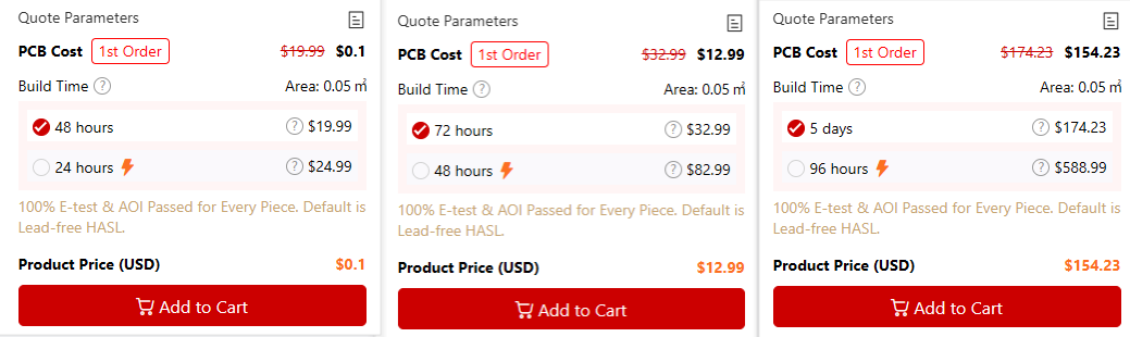
NextPCB 2/4/8-Layer Lead Times based on 5-10 pieces, fr-4 and standard parameters
These are general planning ranges rather than guaranteed delivery times. A manufacturer may offer a shorter quick-turn option for certain designs, while a complex board may require additional engineering review and production time.
For prototype projects, the fastest available service is not always the best choice. If the design requires controlled impedance, unusual materials, microvias, tight tolerances, or special testing, allowing enough time for engineering and quality control can prevent delays later in the project.
Here's a misconception that costs teams days: manufacturing does not begin the moment you place an order.
The production clock starts only after your fabrication data passes engineering review. A CAM engineer must import your Gerbers files and drill files, verify layer alignment, check design rules against the factory's process capabilities, and confirm that all specifications are unambiguous.
For clean, straightforward designs, this review takes two to four hours. For complex boards with controlled impedance requirements, unusual stackups, or incomplete documentation, it can stretch to one to two days. If the review raises questions that require your input, the clock effectively pauses until you respond.
This is why the single most effective way to shorten lead time has nothing to do with paying for expedited service. It's simply providing complete, unambiguous fabrication data from the start. A well-prepared package includes Gerber files for every copper and mask layer, an NC drill file with a tool table, a clear fabrication drawing specifying stackup and impedance targets, and an IPC netlist for electrical testing.
Quick-turn PCB fabrication — accelerated manufacturing with lead times ranging from 24 hours to 7 business days — starts after CAM approval, not after order placement. A job placed on hold for clarification can lose an entire production slot, adding 24 hours or more to your turnaround.
Layer count is one of the most obvious factors. Each additional pair of layers introduces another lamination cycle — a press operation that runs for hours under heat and pressure, followed by gradual cooling to avoid residual stress.
Standard FR-4 is the baseline. When you use common dielectrics and copper weights, fabrication can start immediately — no material validation or special preparation required. Nonstandard configurations may incur 1–2 week lead time delays.
The 2026 supply chain has made this factor more volatile than ever. Standard FR-4 lead times have stretched from the normal 2–3 weeks to 6–8 weeks from major suppliers, while advanced low-loss laminates for high-speed designs now quote 14–18 weeks in some regions. Epoxy resin lead times have increased from around 3 weeks to approximately 15 weeks, and copper foil prices have surged by as much as 30%.
Metal-core PCBs (aluminum or copper base) add another layer of complexity. The base metal, dielectric layer, and mechanical profile all affect thermal performance and manufacturability, making these boards less forgiving than a simple FR4 prototype. Typical metal-core sample lead times run 4–6 days, with mass production at 5–7 days.
If your design specifies a specialty material, confirm availability before you finalize your schedule.
Standard board thickness and copper weight are generally easier to manufacture. A board using standard 1 oz copper is usually simpler to schedule than one requiring several ounces of copper on selected layers.
Heavy copper PCBs require additional plating and etching considerations. Thick copper also changes the manufacturing window for trace width, spacing, hole dimensions, and thermal management. These factors can add days to the schedule — not because the process is fundamentally different, but because each step needs tighter control and more careful handling.
If your design doesn't require heavy copper, sticking with standard weights will keep your order in the faster production queue.
Fine-line designs require tighter manufacturing control. A conventional PCB with relatively generous trace and spacing requirements can normally move through production more easily than a board with very small features.
Very fine traces and spaces may require:
The smaller the design features become, the more important it is to choose a PCB manufacturer with the appropriate process capability. A board that pushes the limits of a fabricator's equipment will inevitably spend more time in review, imaging, and inspection — even if the layer count is low.
Via technology can have a significant impact on lead time.
Standard through-hole vias are relatively straightforward. More advanced structures such as blind vias, buried vias, microvias, and stacked microvias require additional manufacturing processes. HDI PCBs often involve sequential lamination and laser drilling. These additional processes make HDI production more complex than standard multilayer PCB manufacturing.
If your design does not require HDI technology, avoiding unnecessary microvias and sequential build-up can help simplify production.
Check NextPCB Multilayer PCB Stackups & Impedance Control Solutions
Surface finish selection may seem minor, but it directly affects processing hours.
HASL (include Lead-free HASL) is mature and fast. ENIG adds 4–8 hours of processing time compared to HASL due to its multi-step chemical deposition process, though it remains the most common choice for fine-pitch and wire-bondable assemblies. Other options include immersion silver, immersion tin, OSP, and hard gold.
Electrical testing is another fixed time cost. Every board undergoes 100% electrical test — flying probe for prototype quantities under 50 pieces, fixture test for larger batches. Flying probe testing checks every net for continuity and isolation against your netlist, taking 30–90 seconds per board depending on net count. For a 500-board order, that alone can consume significant production hours.
The fabrication sequence itself follows a fixed chain: inner layer imaging and etching, lamination, drilling, plating, solder mask, surface finish, and final inspection. Each step has its own setup time, and setup doesn't compress with order size — it's a fixed overhead.
> Recommend reading: Custom PCB and PCBA Cost Analysis: How to Optimize Design and Reduce Expenses
Testing adds time, but it can be essential for production quality. Depending on the project, a PCB may require:
A prototype with a small quantity may use flying probe testing, while larger production runs may justify a dedicated electrical test fixture.
If a customer requires additional reliability testing or documentation, the final delivery date may also be affected.
Quantity affects production planning in different ways.
A small prototype batch can often be manufactured quickly because it requires relatively little material and production capacity. Larger orders may require production scheduling, additional preparation, and more extensive quality inspection.
However, higher quantities do not always mean proportionally longer manufacturing times. Once production is running efficiently, the cost and time per board can decrease significantly. The setup time — CAM review, tooling, first-article inspection — is a fixed overhead that doesn't compress with order size.
For turnkey assembly projects, component sourcing usually becomes the real bottleneck. One allocated part can add anywhere from 1 to 52 weeks to the schedule. In-stock components from authorized distributors ship in 1–7 days; factory lead time for out-of-stock parts runs 4–12 weeks.
Two PCBs with the same layer count can have very different manufacturing lead times.
A 6-layer board with standard FR-4, conventional vias, and generous design rules may be relatively straightforward — perhaps 7–10 working days.
Another 6-layer board could use:
The second board requires much more process control even though both boards have six layers. Impedance-controlled designs alone add 20–40% to processing time. Boards with tight tolerances — say, ±5% impedance control — require precise control of dielectric thickness, trace geometry, and copper weight, all of which demand slower, more careful processing.
As complexity increases, the DFM review becomes much more intensive. Over-engineering—specifying ultra-tight tolerances or exotic via-in-pad networks when they are not actually required—unnecessarily burns time and escalates CAM and inspection cycles.
Furthermore, when your board must meet IPC Class 3 standards (for high-reliability, aerospace, or medical applications) rather than Class 2 (general industrial), additional inspection and documentation steps enter the timeline. These are not optional shortcuts, but mandatory requirements driven by the reliability target.
> Recommend reading: A Step-by-Step Guide to PCB Fabrication Process
If your project is time-sensitive, you may be considering a quick-turn PCB service.
Quick-turn manufacturing prioritizes production scheduling and is generally intended for prototypes, engineering validation, and urgent development work. A standard prototype may take several business days, while a quick-turn service can sometimes reduce manufacturing time to only a few days. However, quick-turn availability usually depends on the board specifications.
A manufacturer may offer fast production for:
The same manufacturer may need more time for an HDI, rigid-flex, high-frequency, or high-reliability design. When requesting a quick-turn quote, provide the complete PCB specifications rather than asking only for the fastest possible lead time.
| Dimension | Standard | Quick-Turn |
|---|---|---|
| 2-layer FR-4 bare board | 5–7 working days | As fast as 24 hours |
| 4-8 layer multilayer fab | 10–15 working days | 3–5 days (standard materials) |
| HDI prototype | 8–14 working days | 5–8 days |
Sources: NextPCB Quick-turn data
One of the most common sources of confusion is treating production time and delivery time as the same thing.
For example:
The actual shipping time depends on the destination, carrier, shipping method, customs clearance, and whether the manufacturer ships from a domestic or overseas facility.
For overseas PCB orders, always calculate the complete timeline:
Engineering review → Manufacturing → Quality inspection → Shipping → Customs → Delivery
If you have a fixed assembly date, work backward from that date instead of looking only at the manufacturer's production lead time.
If you need PCBs quickly, most delays come down to one thing: something forces the fabricator to stop, ask a question, or add a special process. The strategies below focus on removing those interruptions.
Run a DFM check before you submit. Tools like HQDFM can identify common design issues before files reach the fabricator. Catching a missing drill layer or an annular ring conflict takes seconds; catching it after CAM review costs a day or more.
Use standard materials and stackups. IPC-2221 preferred layer configurations and common dielectrics improve process consistency and eliminate material validation delays.
Keep the design within standard manufacturing rules. Stay within standard manufacturing rules. Avoid unnecessarily tight trace widths, spacing, hole sizes, and tolerances — designs that fit a manufacturer's standard capabilities are easier to schedule. Heavy copper, ENIG, and non-standard finishes add steps; use them only when the design requires it.
Submit complete, consistent manufacturing files. Incomplete or inconsistent files delay engineering review. For a typical order, make sure the manufacturer receives:
Specify impedance, finish, copper weight, and thickness clearly, and keep the fab drawing consistent with the Gerbers — contradictions trigger queries, and every query stops the clock.
Choose the right PCB manufacturer. Not every fabricator specializes in the same technologies. Before placing an urgent order, confirm they can handle your layer count, material, board thickness, copper weight, minimum trace/spacing, minimum hole size, via structure, surface finish, impedance requirements, and testing requirements. A manufacturer with the right capabilities usually offers more predictable lead times than one that has to outsource or add special processes.
Pre-screen your BOM for assembly orders. For turnkey PCBA projects, component availability — not fabrication — is usually the longest pole in the tent. Sharing your BOM and forecast ahead of formal orders creates a path for prioritized allocation.
Place orders earlier in the week. A Friday upload means your CAM review sits idle over the weekend. Monday morning submission starts the clock immediately.
Get Instant PCB & PCBA Quote Online
How long does standard PCB manufacturing take?
Turnaround for a standard order typically runs 7–12 working days, with prototype quantities usually ready faster, in about 5–7 working days. Larger or more complex orders tend to land toward the longer end of that range.
Can I get a PCB made in 24 hours?
Yes — 2-layer FR-4 boards with standard specifications (1.6mm thickness, 1oz copper, HASL finish) are routinely available in 24 hours from major quick-turn fabricators. The clock starts after CAM approval, not after order placement.
Does a more complex board always mean a longer lead time?
Generally yes — more layers, tighter tolerances, or non-standard materials add process steps. But the biggest avoidable delays usually come from incomplete files or specs at the quoting stage, not the board's inherent complexity.
Is lead time the same as delivery time?
No. Lead time is the working days from approved data to the board leaving the factory. Delivery time — transit, customs, and last-mile — sits on top of it. A 7-day lead time plus 3–5 days of shipping means 10–12 days before the board is in your hands.
How can I get my PCBs faster?
Use standard materials and manufacturing specifications where possible, submit complete production files, keep the design within standard manufacturing capabilities, complete DFM checks before ordering, and select a manufacturer with the appropriate production capacity.
PCB lead time is never one number — it depends on layer count, material, copper thickness, design rules, via technology, surface finish, testing, quantity, and overall complexity. A simple 2-layer FR-4 prototype may ship in days; a complex HDI, rigid-flex, or high-reliability board can take weeks.
Look beyond the advertised production time. A reliable schedule includes engineering review, material prep, manufacturing, testing, and shipping. The most predictable delays come from incomplete data and non-standard specs — both of which you control. The least predictable come from raw material markets and component allocation, which you can only manage through early planning and buffer time.
If your project has a fixed deadline, submit complete, unambiguous fabrication data as early as possible. That single habit shortens lead time in every scenario. Everything else follows from there.
Still, need help? Contact Us: support@nextpcb.com
Need a PCB or PCBA quote? Quote now




