



Julia Wu - Senior Sales Engineer at NextPCB.com

 NextPCB Capabilities
Printed Circuit Boards
NextPCB Capabilities
Printed Circuit Boards
 PCB Assembly
 Layer Buildup
 SMD-Stencils
 PCB Design-Aid & Layout
 Mechanics
 Quality
 Drills & Throughplating
 Factory & Certificate
 PCB Assembly Factory Show
Certificate
PCB Assembly Factory Show
Certificate

Support Team
Feedback:
support@nextpcb.com


Black pad is a defect in ENIG (electroless nickel immersion gold) PCBs in which the nickel layer under the gold is corroded during gold deposition. The pad looks normal and may even solder normally at first, but the solder joint forms on a weakened, phosphorus-rich nickel surface and can crack or detach under stress. It is the best-known reliability risk of ENIG, it cannot be seen from outside before assembly, and it is largely a process-control problem that can be reduced by choosing the right finish, specifying inspection and working with a manufacturer that controls its plating baths.
This guide explains what black pad is, how it forms, how to tell it from other soldering defects, how it is detected, how to prevent it and what to do if you suspect it. If you are new to the finish itself, start with the PCB surface finish guide; to compare ENIG with its cheapest alternative, see HASL vs ENIG.
Black pad (also called black nickel or hyper-corrosion of the nickel layer) is damage to the nickel surface of an ENIG finish. In a healthy ENIG pad, a thin gold layer sits on a smooth nickel layer, and the gold dissolves into the solder during reflow so the joint forms with clean nickel. In a black pad, the nickel under the gold has been attacked, leaving a cracked, phosphorus-rich layer. The solder wets the gold normally, but it cannot form a strong metallurgical bond with the damaged nickel, so the joint is brittle.
| Attribute | Black pad |
|---|---|
| Affected finish | ENIG (electroless nickel based finishes); ENEPIG has a much lower risk |
| What happens | The nickel layer is corroded while the immersion gold is deposited |
| Visible before assembly | Usually not; the pad can look normal |
| Typical symptom | Weak joints that fracture at the nickel–solder interface, often found after assembly or in the field |
| Main cause | An uncontrolled or overly aggressive gold or nickel bath |
| Can it be repaired | No; affected boards are replaced |
| Main defence | Process control at the fabricator, plus the right finish and inspection requirements |
ENIG gold is deposited by displacement: gold ions in the bath take the place of nickel atoms at the surface. This reaction should stop once a thin layer of gold covers the nickel. If the gold bath is too aggressive, or the nickel layer is vulnerable, the bath keeps attacking the nickel along its grain boundaries instead.
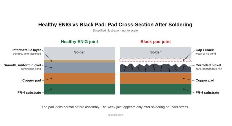
| Stage | Healthy ENIG | Black pad |
|---|---|---|
| Gold deposition | Gold replaces a thin surface layer of nickel, then the reaction stops | The bath attacks the nickel grain boundaries and keeps corroding |
| Nickel surface | Smooth and continuous | Cracked ("mud-crack" appearance) and enriched in phosphorus |
| Soldering | Gold dissolves into the solder; the joint bonds to clean nickel | Solder wets the gold but cannot bond properly to the damaged nickel |
| Joint strength | Strong intermetallic bond | Brittle; fractures at the nickel interface |
| Cause | Why it leads to black pad |
|---|---|
| Overly aggressive or aged gold bath | The bath attacks the nickel instead of stopping once the gold layer forms. |
| Gold bath parameters out of range | pH, temperature and dwell time all change how strongly the gold bath attacks the nickel. |
| Nickel phosphorus content outside the controlled range | A nickel layer that is too low or too high in phosphorus is more vulnerable to attack. Mid-phosphorus nickel is commonly specified. |
| Aged or contaminated nickel bath | A nickel layer deposited from a bath near the end of its life can be porous or uneven. |
| Poor cleaning and activation | Residues on the copper lead to uneven nickel deposition. |
| Insufficient process monitoring | Without regular bath analysis and test panels, drift goes unnoticed until boards fail. |
Black pad is not caused by anything the designer or assembler does in a normal flow. It originates in plating, and that is why the fabricator's process control matters more than any single parameter.
| Problem | Typical symptoms | How it differs from black pad |
|---|---|---|
| Black pad | Joints that fracture cleanly at the pad; a dark, cracked nickel surface exposed on the failed pad | The solder wets the gold normally, so the problem appears after assembly as brittle joints |
| Non-wetting or dewetting from contamination | Solder does not spread, or pulls back from the pad | Visible during soldering and often traced to a contaminated or oxidized pad surface |
| Thin or porous gold | Oxidized nickel; poor wetting after long storage | Shows up as poor wetting before the joint forms, not as brittle fracture |
| Cold solder joint | Dull, grainy joint with poor fillet | A reflow-profile or heating problem, not a plating problem |
| Excess intermetallic growth | Weak joints after heat or aging | Develops over time at the joint; microsection shows an intermetallic layer, not a cracked nickel surface |
The name comes from the dark, rough appearance of the fractured nickel surface when a failed joint is pulled off the board. It does not mean the pads look black before assembly.
| Method | What it shows | Used for |
|---|---|---|
| Microsection (cross-section) analysis | Layer thickness and condition of the nickel–gold interface | Process qualification and failure analysis |
| Scanning electron microscope (SEM) inspection | The cracked, mud-crack nickel surface typical of black pad | Confirming a suspected failure |
| Solderability and wetting tests | Whether solder wets and bonds to the pad | Routine monitoring of plating quality |
| Solder joint pull or shear test | Whether joints fracture at the nickel interface | Checking assembled boards |
| Thickness measurement (X-ray fluorescence) | Nickel and gold thickness | Checking plating is within specification (it does not detect black pad by itself) |
| Bath analysis | Chemistry and phosphorus control of the plating baths | Preventing the problem at the source |
Visual inspection cannot find black pad, and thickness measurement alone does not prove a pad is sound. Reliable detection needs microsection or SEM analysis, which is why controlling the process matters more than inspecting every board.
| Who | Action |
|---|---|
| Fabricator | Control the nickel and gold bath chemistry, temperature, pH and dwell time; keep nickel phosphorus within its range; analyze baths regularly and replace them on schedule; run test panels and microsection checks |
| Designer or buyer | Choose a manufacturer with documented ENIG process control; specify the ENIG gold thickness your design needs; request microsection reports for high-reliability projects; consider ENEPIG for critical or wire-bonded designs |
| Assembler | Check solderability on incoming boards; keep ENIG boards in sealed packaging until use; investigate any joint that fractures at the pad before scaling up an order |
| Factor | ENIG | ENEPIG |
|---|---|---|
| Layers | Nickel, then gold | Nickel, then palladium, then gold |
| Black pad risk | Present if the process is not controlled | Significantly lower, because the palladium layer protects the nickel during gold deposition |
| Wire bonding | Not ideal | Suitable |
| Cost | Lower | Higher |
| Best for | General fine-pitch SMT and BGA | High-reliability designs and wire-bonded boards |
For most fine-pitch designs, well-controlled ENIG performs reliably. If a failure would be very costly, or the board needs wire bonding, ENEPIG removes most of the risk.
| Step | Action |
|---|---|
| 1. Stop | Pause assembly of the affected lot so more boards are not built. |
| 2. Keep samples | Keep failed boards and unassembled boards from the same lot, with date codes and packaging. |
| 3. Analyze | Have the failed pads microsectioned and inspected by SEM to confirm the nickel damage. |
| 4. Contact your manufacturer | Share the lot information and analysis results so they can review the plating records. |
| 5. Decide on the finish | For the replacement lot, consider ENEPIG or ask for tighter inspection requirements. |
Black pad damage cannot be reversed on a finished board, so affected boards are normally replaced.
ENEPIG is available through NextPCB's advanced PCB quote, and ENIG with a selectable gold thickness (1–3 µin in the standard quote, 1–5 µin or custom in the advanced quote) is available in both. Microsection reports are listed among the extras for advanced boards; see the advanced PCB manufacturing capabilities. If your project is high-reliability or high-pin-count, tell your account manager what inspection you need before you order. You can also compare every option on the PCB surface finish options page, or see PCB capabilities.
Black pad is corrosion of the nickel layer in an ENIG finish. During gold deposition the bath attacks the nickel and leaves a cracked, phosphorus-rich layer, so solder joints formed on it are brittle and can fail.
The main cause is an overly aggressive or poorly controlled gold bath. A nickel bath that is aged or outside its phosphorus range, poor cleaning and a lack of process monitoring also contribute.
Usually not. The pad looks normal under the gold. The black, cracked nickel surface is typically seen only after a joint fractures, or in a microsection or SEM image.
Microsection and SEM analysis show the damaged nickel interface. Solderability and joint pull or shear tests give indirect evidence. Visual inspection and thickness measurement alone cannot confirm or rule it out.
No. Black pad is a process-control failure, not a property of ENIG. Boards from a well-controlled ENIG line are reliable and widely used for fine-pitch and BGA designs.
It can be largely prevented by controlling the plating baths, keeping nickel phosphorus within range and monitoring with test panels and microsections. Choosing ENEPIG reduces the risk further.
ENEPIG significantly reduces the risk because the palladium layer protects the nickel during gold deposition, but process control still matters. It also costs more than ENIG.
No. Black pad is specific to electroless nickel based finishes such as ENIG. Immersion silver, OSP, HASL and lead-free HASL do not have a nickel layer. See the OSP guide and HASL vs lead-free HASL.
No. The damage is in the nickel layer under the gold, so affected boards are replaced. Stop assembling the lot and have the failure analyzed.
Pause assembly, keep failed and unassembled boards from the lot, have the pads microsectioned and inspected by SEM, and share the results with your manufacturer.
Choose your finish and gold thickness in the quote form, or ask NextPCB engineers to review your design and reliability requirements.

Still, need help? Contact Us: support@nextpcb.com
Need a PCB or PCBA quote? Quote now

