Arya Li, Project Manager at NextPCB.com

 NextPCB Capabilities
Printed Circuit Boards
 PCB Assembly
 Layer Buildup
 SMD-Stencils
 PCB Design-Aid & Layout
 Mechanics
 Quality
 Drills & Throughplating
 Factory & Certificate
 PCB Assembly Factory Show
Certificate

Support Team
Feedback:
support@nextpcb.com


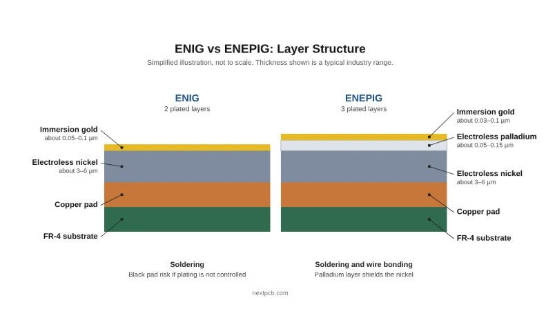
ENIG (electroless nickel immersion gold) is a nickel layer under a thin gold layer. ENEPIG (electroless nickel electroless palladium immersion gold) adds a palladium layer between the nickel and the gold. ENIG is the lower-cost choice for most fine-pitch soldered boards. ENEPIG costs more, but it supports wire bonding, lowers black pad risk and suits high-reliability and mixed-technology assemblies.
This guide compares the two finishes layer by layer, then covers wire bonding, solder joint reliability, cost, storage and how to choose. If you are still comparing all finishes, start with the PCB surface finish guide. For ENIG on its own, read the ENIG PCB surface finish guide, and to compare ENIG with the cheaper HASL option, see HASL vs ENIG.
ENEPIG is a surface finish built from three plated layers on the copper pads: electroless nickel, electroless palladium and a very thin layer of immersion gold. Some sources count the copper and describe it as a four-layer stack. Like ENIG, it gives flat, solderable pads and a long storage life. The difference is the palladium layer, which sits between the nickel and the gold.
The palladium layer does two jobs. During gold deposition it protects the nickel from attack, which is the root of the black pad defect in ENIG. It also gives a surface that works for both soldering and wire bonding, which is why ENEPIG is sometimes called a universal finish.
| Factor | ENIG | ENEPIG |
|---|---|---|
| Layers | Nickel, then gold | Nickel, then palladium, then gold |
| Pad surface | Flat | Flat |
| Soldering | Good, with well-controlled plating | Good, with lower black pad risk |
| Wire bonding | Generally not recommended | Suitable for gold and aluminum wire, depending on layer thickness |
| Black pad risk | Present if the process is not controlled | Significantly lower, though not zero |
| Cost | Lower | Higher, because of the palladium layer and added process step |
| Shelf life | Long, typically about 12 months sealed | Long, typically about 12 months sealed |
| Best for | Fine-pitch SMT, BGA and QFN, general high-quality boards | Wire-bonded boards, mixed-technology and high-reliability assemblies |
| Industry standard | IPC-4552 | IPC-4556 |
In short, choose ENIG when you only need to solder and want the lower cost, and choose ENEPIG when you need wire bonding or want the extra margin against black pad.
| Layer | ENIG | ENEPIG |
|---|---|---|
| Nickel | About 3–6 µm (118–236 µin) | About 3–6 µm (118–236 µin) |
| Palladium | None | About 0.05–0.15 µm (2–6 µin) |
| Gold | About 0.05–0.1 µm (2–4 µin) | About 0.03–0.1 µm (1–4 µin); thicker if gold wire bonding requires it |
These are general industry ranges. The required thickness depends on the standard you design to and on the bonding process, so state your requirement when you request a quote. For ENIG at NextPCB, the gold thickness is selectable in the quote form (see the ordering section below).
Wire bonding connects a bare chip to the board with fine wire, and it is the clearest reason to choose ENEPIG. The palladium and gold layers give a bondable surface for gold wire, and ENEPIG can also support aluminum wire when its thicknesses are suited to the process.
ENIG is generally not recommended for wire bonding. Its thin immersion gold over nickel does not give reliable bonds, and thickening the gold only to fix this adds cost without the other benefits of ENEPIG. If your design uses chip-on-board, bare dies or a mix of soldered parts and wire-bonded dies, specify ENEPIG and tell the engineers your wire type, wire diameter and pad size so they can confirm the layer thickness.
Both finishes solder well on flat pads, and both work with lead-free assembly and multiple reflow cycles. They differ in how the solder joint behaves under stress.
In ENIG, the immersion gold bath can attack the nickel and cause black pad, a brittle, phosphorus-rich nickel layer that weakens the joint. In ENEPIG, the palladium layer shields the nickel from the gold bath, so the risk is significantly lower. It is not zero, because nickel plating quality still matters, so process control by the fabricator remains important. If black pad is a concern for your project, ask your account manager how nickel and gold plating are controlled.
For fine-pitch BGA and other joints you cannot inspect after assembly, this extra margin is the main reason designers pay for ENEPIG.
ENEPIG costs more than ENIG. It adds a palladium plating step and uses a precious metal, and the added cost is higher on small boards, where the process cost is spread over fewer pads and panels. The exact difference depends on board size, quantity and layer count, so the reliable way to compare is to quote the same design with each finish.
For a like-for-like comparison, select ENIG in the standard PCB quote, then request ENEPIG in the advanced PCB quote with the same files and quantity.
Both finishes are stable and keep their solderability for long periods. A typical industry figure for sealed storage is about 12 months for both, but it depends on packaging and storage conditions. Keep boards sealed in their original packaging until assembly, and follow your assembler's storage rules. Neither finish oxidizes like bare copper, so storage is rarely the deciding factor between the two.
| If your board… | Choose | Why |
|---|---|---|
| Is soldered only, with fine-pitch BGA or QFN | ENIG | Flat pads and proven reliability at lower cost |
| Needs wire bonding, alone or with soldering | ENEPIG | The palladium and gold layers give a bondable surface |
| Is used where a joint failure would be very costly | ENEPIG | Lower black pad risk and more margin |
| Combines soldered parts and bare dies | ENEPIG | One finish supports both processes |
| Is cost-sensitive with standard soldered parts | ENIG, or lead-free HASL if pads do not need to be flat | Lowest cost option that still meets the requirement |
| Needs a hard, wear-resistant contact surface | Hard gold | Neither ENIG nor ENEPIG is built for repeated insertion |
For edge connectors and frequently mated contacts, see the PCB gold fingers guide.
ENIG is available in both the standard PCB quote and the advanced PCB quote, with a selectable gold thickness (1–3 µin in the standard quote, 1–5 µin or custom in the advanced quote). ENEPIG is available through the advanced PCB quote, where our engineers review your files. If you need ENEPIG for wire bonding, tell the engineers your wire type and pad requirements before you order. You can also compare every option on the PCB surface finish options page, or see the advanced PCB manufacturing capabilities.
ENIG has two plated layers, nickel and gold. ENEPIG has three, nickel, palladium and gold. The palladium layer makes ENEPIG suitable for wire bonding and lowers the risk of black pad, at a higher cost.
ENEPIG stands for electroless nickel electroless palladium immersion gold. It is a surface finish made of those three plated layers on the copper pads.
ENEPIG plating deposits nickel, palladium and a thin immersion gold layer onto copper pads. It protects the copper from oxidation and gives a surface suited to both soldering and wire bonding.
ENEPIG is the standard name and uses an electroless palladium layer. ENIPIG, with an immersion palladium layer, is a related variant that some suppliers use. Ask your manufacturer which process they run if the palladium type matters to your design.
ENIG uses gold and nickel deposited through several tightly controlled electroless steps, so it costs more than HASL or OSP. ENEPIG adds a palladium layer, so it costs more than ENIG. Compare finishes in the quote form to see the difference for your design.
It depends on the design. ENEPIG is better for wire bonding and for high-reliability boards where black pad risk matters. For boards that are only soldered, well-controlled ENIG performs reliably and costs less.
Yes. ENEPIG adds a palladium layer and an extra process step. The difference varies with board size and quantity, so quote the same design with both finishes to compare.
ENIG is generally not recommended for wire bonding because its thin immersion gold does not give reliable bonds. ENEPIG is the usual choice when a board needs both soldering and wire bonding.
No, but it reduces the risk significantly. The palladium layer protects the nickel during gold deposition. The quality of the nickel plating still matters, so the fabricator's process control remains important.
ENEPIG is used for boards that are wire-bonded, boards that combine soldered parts and bare dies, and high-reliability assemblies with fine-pitch BGA or other joints that cannot be inspected after assembly.
The ENEPIG plating itself contains no lead. Whether an assembly is RoHS-compliant also depends on the solder and components used, so confirm your requirement with your manufacturer.
Yes. ENEPIG is available through the advanced PCB quote, where engineers review your files. ENIG is available in both the standard and advanced PCB quotes.
Choose ENIG in the instant quote form, or request ENEPIG through the advanced PCB quote and have our engineers review your wire bonding and reliability requirements.

Still, need help? Contact Us: support@nextpcb.com
Need a PCB or PCBA quote? Quote now