
 NextPCB Capabilities
Printed Circuit Boards
NextPCB Capabilities
Printed Circuit Boards
 PCB Assembly
 Layer Buildup
 SMD-Stencils
 PCB Design-Aid & Layout
 Mechanics
 Quality
 Drills & Throughplating
 Factory & Certificate
 PCB Assembly Factory Show
Certificate
PCB Assembly Factory Show
Certificate
Support Team
Feedback:
support@nextpcb.com


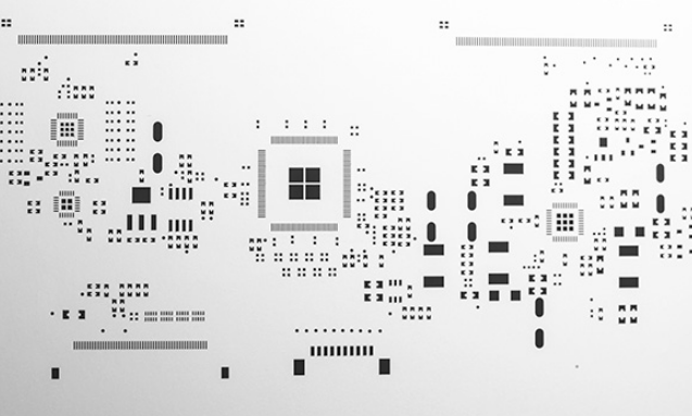
Stencil PCB is a stainless steel foil on which laser-cut holes correspond to component pins on the PCB's surface. It plays a vital role in providing solutions in manufacturing industries. After the proper alignment of the board on the PCB stencil, you can pull solder paste through the Stencil to fill in the Stencil's holes. The PCB stencil's sole purpose is to transfer wet lead to the bare board. The amount of damp information entering the board determines by the thickness of the stainless steel foil and the opening size. This SMT stencil technology has high scope due to its speed, reliability, and low cost compared to other primitive methods.
Surface Mount Technology, also known as SMT, produces electrical components that involve mounting the components directly on the surface of a Printed Circuit Board (PCB). SMT's relevance has gone a long way toward replacing the previous electronic component production format, Through-Hole Technology.
With an SMT or PCB stencil, you can evenly spread solder paste on a circuit board before selling the PCB components. Previously, the board's stainless steel foil created an opening for each part attached to it. When you remove the stainless-steel foil from the board, the solder paste remains, and you can adhere it to the circuit board using the SMT stencil. Surface Mount Devices are devices manufactured by SMT technology.
Categories of pcb stencils
Based on the solder paste application, you can find the mentioned types as explained below:
Frameless Stencils
This solder paste SMT stencil is ideal for use with stencil tensioning systems.
Some of the benefits of this tool are:
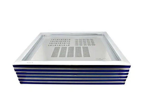
Framed Stencils
This SMT stencil also functions as a glue-in stencil with a permanent frame. Furthermore, the frame or mesh border provides maximum precision by stretching the foil.
The following advantages come with this framed Stencil:
PCB stencil dimensions consist of two parts: internal dimensions and overall dimensions. The internal size is the size that is compatible with the PCB ready to be assembled, while the overall size is the size that is compatible with the parameter limitations of the printing machine. By accurately designing both dimensions, the stencil will be able to fully utilize its function.
The internal dimensions of a stencil can be calculated according to the following rules: width of a framed stencil = width of the PCB + 100mm and its length = length of the PCB + 100mm.Width of frameless stencil = width of PCB + 200mm and its length = length of PCB + 200mm.
For example, if a board size is 50*50mm, then its framed stencil size should be around 150*150mm and frameless stencil size should be around 250*250mm. It is easy to memorize and operate, so it is suitable for SMT assembly before the appearance of automatic printing machine.
Before the advent of automatic printing machines, it is suitable for manual solder paste printing in SMT assembly. It can be said that different PCB sizes lead to the creation of stencils with different internal dimensions.
However, when it comes to automatic solder paste printers, it is relatively reliable. The overall size of the stencil has to be determined by the parametric limits of the device, i.e. the printing press, as the stencil has to work within the confines of the printing press band frame. Different presses have different parameter regulations. As far as PCBCart is concerned, the stencil size compatible with our presses can be 650mm*650mm or 736mm*736mm.
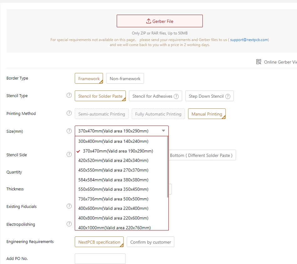
Above are the common pcb stencil sizes for nextpcb, order now!
Still, need help? Contact Us: support@nextpcb.com
Need a PCB or PCBA quote? Quote now


 Surface

