
 Surface


Julia Wu - Senior Sales Engineer at NextPCB.com

 NextPCB Capabilities
Printed Circuit Boards
NextPCB Capabilities
Printed Circuit Boards
 PCB Assembly
 Layer Buildup
 SMD-Stencils
 PCB Design-Aid & Layout
 Mechanics
 Quality
 Drills & Throughplating
 Factory & Certificate
 PCB Assembly Factory Show
Certificate
PCB Assembly Factory Show
Certificate
Support Team
Feedback:
support@nextpcb.com


Table of Contents
Semiconductor devices are fundamental to modern electronics, utilizing the unique electrical properties of semiconductor materials to precisely control electric current. An authoritative definition describes a semiconductor device as an electronic component whose conductivity lies between that of a conductor (like copper) and an insulator (like glass). It functions by controlling charge carriers (electrons and holes) to achieve rectification, amplification, switching, sensing, or photoelectric conversion. These devices conduct electricity in a solid state, a key difference from vacuum tubes, which has led to significant reductions in size, power consumption, and increased reliability of electronic components.
The strength of semiconductor materials lies in the ability of engineers to manipulate their electrical behavior through sophisticated methods. The primary methods include doping, which involves the deliberate addition of impurities (such as Phosphorus or Boron) to increase the number of free electrons or holes; and applying electric fields, light, or heat to change the material’s conductivity. By precisely controlling the location and concentration of these doped regions, engineers can fabricate billions of tiny functional units, such as diodes and transistors, on a single silicon wafer, forming the basis of modern integrated circuits (ICs).
Semiconductor devices are irreplaceable, acting as critical components driving modern society. From the Central Processing Units (CPUs) in personal smart devices to the Radio Frequency (RF) front-ends in global communication networks, from power inverters in electric vehicles to industrial automation control systems, virtually all electricity-dependent applications rely on semiconductor devices. They are essential not only for complex computation and communication but also for efficient energy conversion and management.
Band Theory: The fundamental reason for conductivity differences lies in the material's energy band structure. Semiconductors possess a moderate Bandgap (Eg), allowing electrons to be excited into the conduction band to conduct current at room temperature, whereas insulators have energy gaps that are too large. Band theory sets the physical limits for designing devices that tolerate high voltage and high temperature.
Doping and PN Junction: Through doping processes, semiconductor material is categorized into N-type (majority carriers are free electrons) and P-type (majority carriers are holes). When N-type and P-type semiconductors are joined, a PN junction is formed. A region naturally depleted of free carriers, known as the Depletion Region, forms at the junction, creating a built-in electric field, or natural voltage barrier.
PN Junction: The Current Switch/Control Element: The PN junction is the foundation for all rectification and switching functions. Applying an external voltage (bias) controls the width and height of the depletion region, thereby determining whether current can flow. When a forward bias voltage exceeds the built-in barrier (e.g., approximately 0.7V for Silicon), the depletion region narrows sharply, and current increases exponentially.
Electric Field Control (FET) vs. Current Control (BJT): This is the key distinction between the two major classes of transistors.
> Recommend reading: What's the difference between MOSFET and BJT and how to choose?
The material's bandgap (Eg) dictates the electrical and thermal limits of the device. First-generation Silicon (Si), with its mature processes and low cost, remains dominant, but its 1.12 eV bandgap constrains its performance in high-voltage, high-temperature, and high-frequency applications.
Third-generation Wide Bandgap (WBG) materials, such as Silicon Carbide (SiC, ≈ 3.3 eV) and Gallium Nitride (GaN, ≈ 3.4 eV), possess a critical electric breakdown field (Ec) several times higher than that of Si. This high Ec is essential for achieving breakthroughs in power device performance. In traditional Si devices, increasing the breakdown voltage (BV) requires thickening the semiconductor drift region, which inherently increases the on-state resistance (Rds(on)) and conduction losses. WBG materials solved this trade-off: they allow engineers to design devices with significantly higher voltage tolerance (BV) but thinner drift regions, thereby achieving remarkably low Rds(on) while maintaining high voltage ratings. This is the fundamental reason SiC/GaN achieve high efficiency in high-power applications.
Forward Bias: The external voltage is applied in the opposite direction to the internal barrier. When the external voltage reaches or exceeds the barrier voltage (approx. 0.7V for Si), the depletion region narrows sharply, allowing majority carriers to flow, and the device turns ON.
Reverse Bias: The external voltage is applied in the same direction as the internal barrier. This widens the depletion region and increases the barrier height, blocking current flow, and the device is in the OFF-state, with only a tiny reverse saturation current flowing.
Diode I–V Exponential Law: The current-voltage relationship of an ideal diode is exponential: I = I0 (e^(qV/nkT) − 1). This exponential dependency makes the device highly sensitive to temperature variations.
MOSFET I–V Region Concepts:
The semiconductor device family is vast, with core differences in structure, carrier type, and control mechanism.
| Device Type | Control Method | Typical Function/Application | Key Characteristic/Advantage |
|---|---|---|---|
| Diode | PN Junction/Light/Bias (Uncontrolled) | Rectification, Voltage Reference, Photoelectric Conversion | Unidirectional conductivity, Schottky near-zero trr |
| Bipolar Junction Transistor (BJT) | Current Control (IB) | Analog Small-Signal Linear Amplification | High transconductance, excellent linearity |
| Field-Effect Transistor (FET) | Voltage Control (VGS) | High-Speed Switching, Digital Logic, Current Amplification | Extremely high input impedance (Zin), unipolar operation |
| Power Switch (IGBT/MOSFET) | Voltage Control (VGS) | High Power, High Voltage/High Frequency Switching | Low Conduction Loss (Rds(on)) or Low Switching Loss (Qg) |
| Thyristor | Gate Pulse Trigger (Latching) | High-Power AC Control, Rectification | Unique latching characteristic, high current capacity |
| RF/Microwave Device (HEMT) | Voltage Control (VGS) | Millimeter-Wave Amplification, High-Frequency Power | Extremely high electron mobility (2DEG), extremely high operating frequency |
| Sensing and MEMS | Environmental Physics (Light, Heat, Pressure, Gas) | Conversion of Physical/Chemical quantities to Electrical Signals | Based on conductivity changes, IC compatible |
> Recommending reading: Introduction to Printed Circuit Board Diode (PCB Diode)
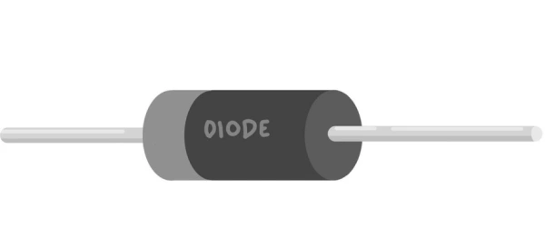
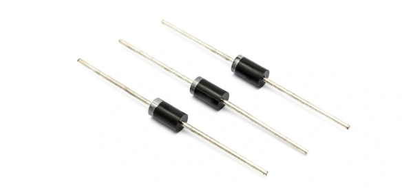
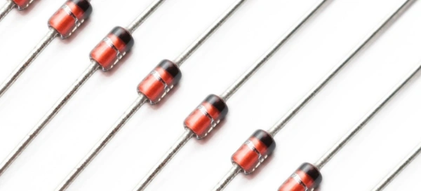
Rectifier Diode: The classic PN junction structure, primarily used to convert alternating current (AC) to direct current (DC) in line-frequency or mid-frequency circuits, often featuring high breakdown voltages (typically 200V to 1000V).
Schottky: Formed by a metal-to-N-type semiconductor contact, operating as a unipolar device. Its core advantage is a very low forward voltage drop (VF). The Schottky diode generates virtually no minority carrier reverse recovery (trr is negligible), though it is not strictly zero and is still affected by junction capacitance. This characteristic significantly reduces high-frequency recovery losses, making it the preferred choice for secondary rectification in low-voltage, high-frequency switching power supplies.
Zener: Uses a heavily doped PN junction, specifically designed to operate stably in the reverse breakdown region. Commonly used as a voltage reference or in voltage clamping protection circuits, leveraging its stable reverse breakdown voltage characteristic.
Photodiode / Solar Cell: Utilizes the photovoltaic effect in semiconductor materials, absorbing photons to generate electron-hole pairs, converting light energy into electrical energy.

LED / Laser Diode: Current injection across a forward-biased PN junction causes carriers to recombine, emitting light (electric-to-light conversion). LEDs primarily rely on spontaneous emission and cover a power range from milliwatt to multi-watt for lighting and displays. Laser diodes rely on stimulated emission, producing coherent, high-power-density light beams. Widely used in optical communication, measurement, and storage (e.g., CD/DVD).

BJT is a current-controlled device, involving the transport of two types of carriers (electrons and holes), hence bipolar.

Features: BJTs use an NPN or PNP three-layer structure and feature high transconductance. When operating in the Active Region, they can provide highly linear current amplification.
Application: Primarily used for small-signal amplification, current mirrors, and precise linear signal processing in the analog circuit front-end. Engineers establish a stable quiescent operating point (Q-point) to ensure low-distortion signal amplification.
FETs are voltage-controlled devices, relying solely on majority carriers for conduction (unipolar), and feature high input impedance.
> Recommend reading: What Is an FET (Field-Effect Transistor)?
MOSFET (Core): Features an insulated gate structure (Metal-Oxide-Semiconductor), with extremely high input impedance (up to 1014 Ω). Due to superior switching characteristics and ease of large-scale integration, MOSFETs are the dominant device in digital logic and power electronics.
> Recommend reading: IRFZ44N: The Ultimate Guide to This Powerful MOSFET Transistor
JFET: The gate is formed by a PN junction, resulting in high input impedance (typically 109 Ω, lower than MOSFETs). JFETs excel in low-noise amplification and specific analog applications requiring superior linearity.
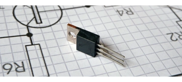
Power MOSFET (Si): Silicon MOSFET solutions are mature across low voltage to medium-to-high voltage (including 600V–900V Super Junction) applications. Above 400V, device selection is typically a trade-off between SJ MOSFET / IGBT / SiC based on switching frequency and loss targets. Si MOSFETs excel at high-frequency switching (>100 kHz) due to their low Rds(on) advantage.
IGBT (Insulated Gate Bipolar Transistor): Suitable for medium-to-high voltage (typically >400V) and high-current industrial applications, such as motor drives. The IGBT combines the voltage control of the MOSFET with the high current density of the BJT. Its drawback is the Tail Current during turn-off, caused by the slow recombination of minority carriers, which severely limits its switching frequency (usually below 20 kHz).
Wide Bandgap Devices (SiC / GaN):
Features: The Thyristor (SCR, Silicon Controlled Rectifier) is a PNPN four-layer structure device. Its unique feature is the latching characteristic: once triggered into conduction by a gate pulse, the device remains ON even if the gate signal is removed, provided the anode current does not drop below its Holding Current.
Application: Primarily used for high-power rectification, AC power control (such as soft-start, dimming), and industrial power supplies. The TRIAC (TRIode for Alternating Current) is a variant of the SCR capable of controlling both half-cycles of AC current.
HEMT / pHEMT, GaAs/GaN Devices: High Electron Mobility Transistors (HEMTs) form a Two-Dimensional Electron Gas (2DEG) at the junction interface between materials with different bandgaps (heterojunction, such as AlGaN/GaN), providing extremely high electron mobility.
Application: HEMTs can operate at millimeter-wave frequencies and are used in high-frequency front-ends, base stations, radar, and satellite receivers. GaN HEMTs offer superior performance over traditional GaAs devices in microwave wireless communication (e.g., 5G power amplifiers) due to their higher critical electric field and power density.
Fundamental Principle: Semiconductor sensors utilize the sensitivity of semiconductor materials to environmental stimuli (e.g., temperature, pressure, gas concentration, light) to convert physical or chemical quantities into measurable electrical signals. Their operation is based on changes in electrical conductivity or resistance. > Analysis of the future development trend of sensors
Types and Basis:

After the selection and circuit design of semiconductor devices are finalized, the critical step of translating the design into a reliable product lies in supply chain management and manufacturing. NextPCB provides a Turnkey PCB Assembly service, assisting engineers with a smooth transition from prototype design to mass production.
Customers only need to provide Gerber files and the Bill of Materials (BOM) list to execute the entire process of PCB fabrication, component procurement, and precision assembly. This model significantly simplifies project management, offering the advantage of a single supplier interface.
Upload & Get BOM Service at NextPCB
Core Manufacturing and Assembly Capabilities:
Try HQDFM Online Get Free DFM/DFA Analysis
| English/Abbreviation | Definition |
|---|---|
| Bandgap | The energy difference between the conduction band and the valence band, determining the semiconductor material's intrinsic electrical properties and temperature tolerance |
| Doping | The process of intentionally introducing impurity atoms into a semiconductor crystal to precisely control its majority carrier type and concentration |
| PN Junction | The interface connecting P-type and N-type semiconductors, forming the fundamental structure of diodes and transistors |
| Breakdown Voltage (BV) | The maximum voltage the device can withstand in the reverse-blocking mode, a crucial limit for reliability design |
| Rds(on) | The equivalent resistance between the Drain and Source when the MOSFET is fully conducting, used to calculate conduction loss |
| Gate Charge (Qg) | The total electrical charge required to turn a field-effect device (MOSFET/IGBT) ON or OFF, a key parameter determining switching speed and drive power |
| Reverse Recovery (trr) | The time required for minority carriers to be cleared when a bipolar device (like a PN diode or IGBT body diode) switches from conducting to blocking, a major source of high-frequency loss |
| SOA (Safe Operating Area) | The region defined by voltage and current combinations where the device can safely operate under specified conditions and temperature |
How to quickly distinguish between MOSFET and IGBT?
Distinction Dimension: IGBTs are better suited for handling high voltage (>400V) and large currents, with low conduction loss, but their switching frequency is generally limited to below 20kHz due to minority carrier effects. MOSFETs excel at low voltage (<250V) and high frequency (>100kHz), with extremely fast switching speed. For high-frequency applications above 600V, SiC MOSFETs should be considered.
What is the intuitive difference between SiC and GaN?
Distinction Dimension: SiC is stronger in voltage and current handling capability (>600V, high current), making it the preferred choice for high-voltage, high-current industrial and automotive applications. GaN offers advantages in extremely high frequency (MHz range) and ultimate power density, suitable for medium-to-low voltage high-frequency switching, such as consumer fast chargers and high-frequency DC/DC converters.
Why is the Schottky diode more "power-saving"?
The Schottky diode is a unipolar device that does not rely on minority carriers for conduction. Consequently, it has a very low forward voltage drop (VF), significantly reducing conduction loss. Crucially, it has no reverse recovery time (trr), eliminating recovery loss during high-frequency switching and thus achieving higher efficiency.
Semiconductor devices are the backbone of electronics, with their performance dictated by material science, precise physical structure, and stringent manufacturing processes. When selecting a device, engineers must cross-match the "three essential elements" (voltage, current, and frequency) with the four key parameters (BV, Rds(on), Qg, Rth).
The power electronics sector is currently undergoing a major transformation driven by SiC and GaN. Wide bandgap materials have overcome the inherent trade-off between conduction loss and switching loss found in traditional Si devices for high-voltage and high-frequency applications. This enables system designs to achieve higher efficiency and unprecedented power density. In the future, as the manufacturing costs of WBG devices decrease and the supply chain matures, they are expected to take central roles in high-growth areas such as electric vehicles, data centers, and renewable energy, pushing the entire electronic system toward smaller, faster, and more efficient development trends.

Still, need help? Contact Us: support@nextpcb.com
Need a PCB or PCBA quote? Quote now

