

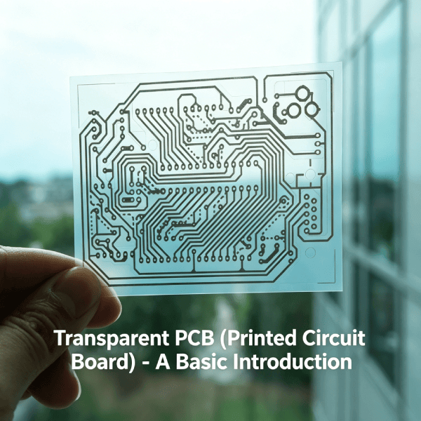
 NextPCB Capabilities
 PCB Assembly
 Layer Buildup
 SMD-Stencils
 PCB Design-Aid & Layout
 Mechanics
 Surface
 Quality
 Drills & Throughplating
 Factory & Certificate


-

-
-
Understanding Signal Integrity in PCBs
The quality of the signal traveling over a transmission line is known as signal integrity.
6632 3 0 Shares
-
Acid Traps
Acid traps are sharp turns and corners in PCB trace patterns that can retain the chemicals used for PCB etching
11366 8 0 Shares
-
-

-
-
-
-
-
-
-
-
-
-
-
-
-
-
Important IPC Standards for PCB Manufacturing
This article introducts the importance, performance classed of IPC standard for PCB manufacturing.
7051 1 0 Shares

Categories
Recommended Article:
- Shielded vs Unshielded Inductors: EMI Impact and PCB Placement Best Practices
- Common Mode Choke: How It Works, PCB Layout Rules and Differential Pair Applications
- Ferrite Bead vs Inductor: When to Use Each for EMI Filtering in PCB Design
- Power Inductor Selection Guide: Inductance, DCR & PCB Footprint
- MLCC Piezoelectric Effect: Acoustic Noise, Microphonics and How to Mitigate in PCB Design
- Bulk vs Decoupling Capacitor: The Three-Tier Capacitor Strategy
- ESR and ESL in Capacitors: What They Mean and Why They Matter in PCB Power Integrity
- Film Capacitor vs Ceramic Capacitor: Applications, Trade-offs and PCB Layout Considerations
- MLCC 0402 vs 0201 vs 0603: Size Selection Guide for High-Density PCB Assembly
- Tantalum Capacitor vs MLCC: When to Use Each in Your PCB Design