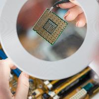
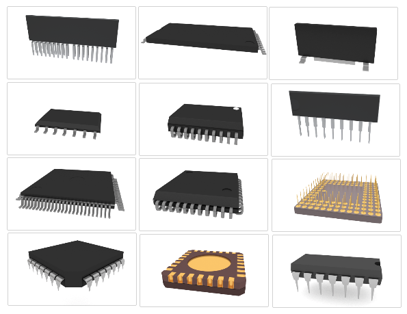
Top 9 Most Common IC Packaging Types in Modern Electronics
In modern electronic products, IC (Integrated Circuit) packaging types play a crucial role in performance, reliability, and cost. This article introduces the eight most common IC packaging types, including PGA, DIP, QFP, BGA, and more, which are widely used in various electronic devices. Understanding these packaging types helps designers and engineers make more informed choices to meet the specific needs of different products.


 NextPCB Capabilities
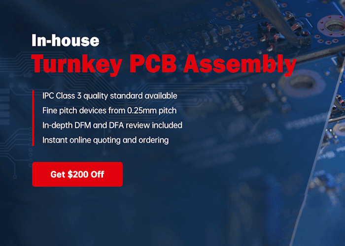
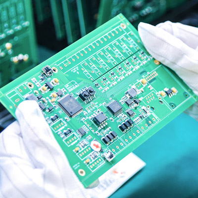
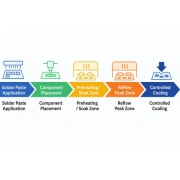
 PCB Assembly
 Layer Buildup
 SMD-Stencils
 PCB Design-Aid & Layout
 Mechanics
 Surface
 Quality
 Drills & Throughplating
 Factory & Certificate