
 NextPCB Capabilities
Printed Circuit Boards
NextPCB Capabilities
Printed Circuit Boards
 PCB Assembly
 Layer Buildup
 SMD-Stencils
 PCB Design-Aid & Layout
 Mechanics
 Quality
 Drills & Throughplating
 Factory & Certificate
 PCB Assembly Factory Show
Certificate
PCB Assembly Factory Show
Certificate
Support Team
Feedback:
support@nextpcb.com


A 12-layer PCB stack-up is a sandwich-like structure of an electronic circuit consisting of three different materials Copper, Prepreg and substrate. In a stack-up, conducting layers of a PCB are placed one by one, separated with a layer of prepreg, baked and pressed at a high temperature to bind together and make a firm structure PCB.
The stack-up of a PCB determines the thickness, weight and size of the PCB.
The three materials used in a 12-layer PCB stack-up are
Copper: Copper is the conducting material of a PCB. The signal traces consist of copper.
Prepreg: Prepreg is an isolating material sandwiched between core and copper layers. The primary function of prepreg is to bind two cores or one core with a copper layer.
Core/Substrate/Base Material: A dielectric material used for mechanical support and isolation. The Core is a laminate pre-coated with copper on both sides.
A 12-layer PCB stack-up involves the arrangement of the conducting and insulating layers of the PCB.
A stack-up design is necessary for fulfilling the electrical requirements of a circuit board in a precise way. Hence, it is done by an engineer who considers all aspects of the circuit to produce a perfectly functioning board. To simplify this complex process, you can refer to pre-verified impedance control stackups for optimized layer arrangements.
On a general basis, a 12-layer PCB stack-up should facilitate at least five cores and six layers of prepregs. The designers decide the number of Power and Ground layers on the stack-up designing stage. The number of planes on a 12-layer PCB decides on the base of isolating and electromagnetic compatibility (EMC is the ability of a circuit or system to work appropriately under electromagnetic interference) requirements of the board.
Briefly, the concept of designing a 12-layer PCB stack-up is to provide good opportunities to route high-speed, high-frequency and mixed signals.
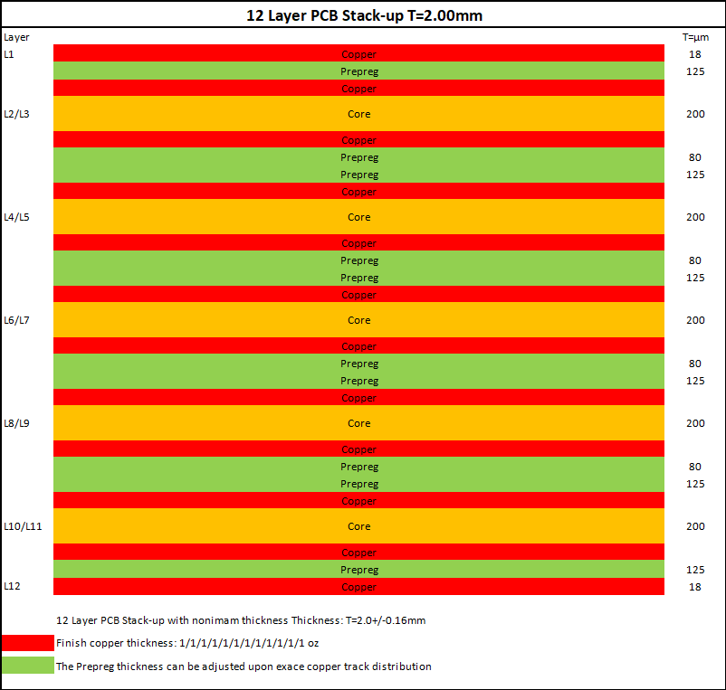
A standard 12-layer PCB stack-up has 12 conductive (copper) layers for signal traces separated by five layers of core and six layers of prepregs. To aid your learning and knowledge about the standard 12-layer PCB stack-up, here we are explaining stack-up options comprised of the standard thickness of materials.
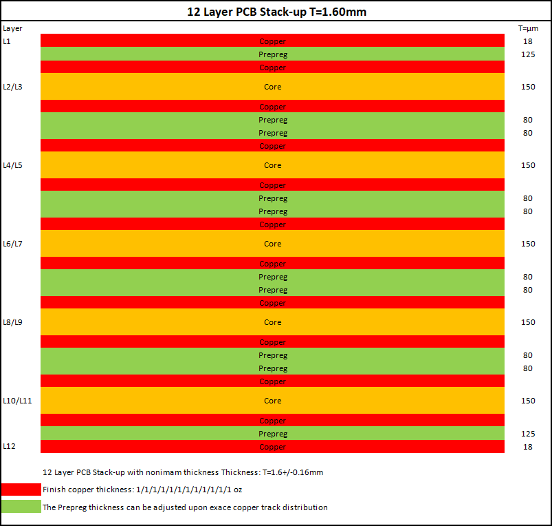
In this stack-up, there are three Power planes, three Ground planes and six signal layers to route signal tracks. Each layer signal layer is adjacent to a plane, which increases the isolation among the signal layers and reduces cross-talk. This stack-up provides an adjacent ground and power plane at L10 and L11, which makes the L12 (due to higher isolation) perfect to route analogue signals.
To make a circuit compatible with the electromagnetic environment and prevent the effects of the external electromagnetic environment on its performance, the designers may avail the opportunity of dedicating the outermost layers as the Ground plane. This stack-up has a Ground and Power plane adjacent to each signal layer that reduces the volt drop and ensures shorter current return paths, better heat dissipation and higher current handling capacity.
The standard thickness of a 12-layer PCB is 1.6mm. However, this is not a fixed value, but it is the most used thickness for a 12-layer PCB.
A Standard value does not necessarily suit every type of circuit. Some PCBs require thicker materials for several purposes. For example, to increase mechanical strength or isolation among the layers.
A 12-layer PCB, due to its increased surface, provides several advantages and disadvantages. Some of them are as follows.
Pros of a 12-Layer PCB
A 12-layer PCB provides a large number of layers that make the process of routing complex signals easy.
On a 12-layer PCB, the designers usually have 3 Power planes that reduce the volt drop in the circuit.
In a 12-layer PCB, almost every signal layer is adjacent to a plane. Hence, it provides adequate isolation and shorter current return paths.
A 12-layer PCB has a higher capacity to deal with an electromagnetic environment, which makes it superior to use under a high electromagnetic environment.
To tolerate higher heat stress, a 12-layer PCB allows heat sinks to be used, which makes heat dissipation faster.
The 12-layer PCB has a higher number of prepregs, core and conducting layers, which makes it thicker and denser. Hence they provide good performance against mechanical stress.
A 12-layer PCB provides considerable space to route signals, but the disadvantage of this PCB is that we can route complex circuits in internal layers, but we have small surface-to-place components on external layers.
The 12-layer PCBs are complex and usually have lots of signal traces on internal layers that are hard to troubleshoot and modify once the PCB is manufactured. To deal with this situation, the designers should place a short piece of the signal tracks on an external layer so that if they need to modify that individual track, they can easily cut it and fixed with wires etc.
Due to the complexity of a 12-layer PCB, the designers and manufacturers charge more than an 8-layer or 10-layer PCB. But if the design of the circuit firmly demands a 12-layer PCB, it is worth investing in it.
The typical thickness of a 12-layer printed circuit board range from 1.6mm to 2.4mm and further depend on the requirements of the PCB. In a PCB, the thickness of the copper layer, prepreg and core determine the final thickness. For example, if a circuit requires extra isolation among the signal layers or needs additional mechanical strength, it will use a thicker prepreg and core. This increase in the thickness of the material will add up to the overall thickness of the PCB.
Mainly five factors affect the cost of a 12-layer PCB. They include
High-quality material is the priority of each circuit. But some designs demand extra efficient materials, such as high-frequency and high-speed PCBs require high-frequency laminates (core). Such laminates are higher in cost. The extra efficient material increases the price of the PCB with each increasing layer. Further, a large PCB requires more material and manufacturing time, so it is also an important factor to consider when determining the cost of the PCB.
If a PCB operates a large amount of current, it requires wider and thicker signal traces to avoid excess heat production when the current flows through the circuit. In a 12-layer PCB, there are 12 conducting layers used, and increasing the thickness of each layer may affect the budget of a PCB.
The PCBs that operate at higher temperature and generates high heat during the operation requires a higher glass transition temperature. The manufacturers increase the glass transition temperature of the PCB by modifying its resin. For this special process, the manufacturers charge extra.
The quantity and size of the holes present on a PCB are one of the major factors that determine its price. A large amount of holes requires more time to drill, especially holes with smaller diameters requiring special machinery to drill. Further on the electroplating level, these holes need more conducting material to deposit onto them. All these factors affect the cost of a PCB and its manufacturing time.
All the factors mentioned above affect the price of a PCB. However, if a PCB has some other unique specifications, it may also fluctuate in cost of the PCB. Because PCBs, with special requirements, require special machinery and labour attention to fabricate them.
A 12-layer PCB has several applications in different industries. But the main applications of 12-layer PCBs are in
A reason for the popularity of the 12-layer PCB stack-up is that it provides considerable space to route complex designs. In a 12-layer PCB stack-up, the designers can easily divide the layers into planes and signal layers. This division of layers helps to achieve maximum isolation and reduce cross-talk and electromagnetic interference (EMI) issues.
In a 12-layer PCB stack-up, the designers have the opportunity to play with the Ground and Power plane. The average number of power planes we can adjust in a 12-layer PCB is three. In most cases, this number of power planes is enough to route power traces without volt drop.
The 12-layer PCB stack-up is also famous for its electromagnetic compatibility. Usually, medical and laboratory devices experience a high electromagnetic environment, which affects the performance of the PCB and creates electromagnetic interference among the signals. The electromagnetic compatibility of a 12-layer PCB is another reason for its hype.
The fabrication process of a 12-layer PCB consists of several steps. It includes
It is the most important and foremost step in the manufacturing process of a 12-layer PCB. In this step, the designer finalizes the thickness of the material and arrangement of the signal layers, Ground and Power planes. After designing the stack-up, the designer works on the layout of the board.
Phototools are individual negatives of each layer of the PCB. In this process, the manufacturer used a UV plotter to convert the digitally designed layers of the PCB into films known as phototools.
It is the process of converting (printing) phototools onto the pre-coated copper laminates. After printing the phototool on the laminates, a coat of photoresistive material is applied and hardened through UV light.
In this step of the 12-layer PCB manufacturing, the unhardened copper is etched and removed through pressure washing.
It is necessary to take care of the internal layers of the PCB because once all the layers are bound, it is impossible to make changes in the inner layers. This process of verifying the layers of the PCB is automatic. After the inspection, the same laminates go for drilling vias and holes.
Once the inspection and holes are done, the PCB layers are stacked, pressed and baked at high temperature to melt the prepregs to bind cores and copper layers together.
After binding the layers, the final structured PCB goes for external hole drilling.
As soon as the drilling of the vias and holes is complete, the final stack-up needs electroplating to deposit some conducting material on the walls of drilled holes to make them conductive.
The preparation of outer layers repeats the same process as inner layers.
The solder mask is a non-conducting liquid resin material applied to ensure that there are no shorts among the signal traces.
Silk screening is the process of printing relevant information on the PCB.
The last step of the manufacturing process of a 12-layer PCB is testing the PCB against the actual layout file.
To read the fabrication process of a 12-layer PCB in detail, please read this article. The fabrication process of a standard multilayer PCB is the same as the manufacturing process of a high-frequency PCB.
The function of a heat sink is to conduct heat and spread it on its large surface to boost the process of heat dissipation. A 12-layer PCB usually has applications in complex circuits that either generate an excessive amount of heat or operates at high temperature. In both cases, heat damages components and affects the overall performance of a printed circuit board.
A 12-layer PCB routes complex designs and uses semiconductor chips with the earliest technologies. Some microchips and microcontrollers operate with very high currents and generate a large amount of heat. The designers place a heat sink on these chips to dissipate the heat generated by the semiconductor chips at a faster rate.
Hence, concerning mechanical strength and electrical requirements, a 12-layer PCB is compatible to include a heat sink.
NextPCB is one of the experienced manufacturers of 12-layer PCBs all around China, providing high-quality PCB products with dedicated customer service. We have been manufacturing single-layer to multilayer boards for more than 15 years. Our experience and quality of work have given us the confidence to count Next PCB as one of the best 12-layer PCB manufacturers around the globe. We are manufacturing all the 12-layer PCB stack-ups written above and other stack-ups provided by our honourable clients.
The other services of Next PCB include components sourcing, PCB prototyping/PCB manufacturing, PCB assembly, quality testing, and the final shipment. Briefly, NextPCB can meet all your PCB requirements, from PCB prototyping to small or mass PCB production.
>>Get a quick online PCB quote within 24 hours<<
A 12-layer PCB stack-up provides twelve conducting layers to route signal traces. These twelve layers divide into signal layers, Ground and Power planes. The average number of planes that we can have in a 12-layer PCB is 5-6; the rest of the layers are dedicated to routing the signal traces.
The higher number of Ground and Power planes in a 12-layer PCB provides maximum isolation among the signal layers, eliminates cross-talk, and reduces electromagnetic interference (EMI) issues.
A 12-layer PCB provides electromagnetic compatibility and interplane capacitance, which eliminates internal and external electromagnetic interference among the signals. This feature of a 12-layer PCB ensures signal integrity and maximum shielding and provides better opportunities to route high-frequency, high-speed and mixed signals.
The 12-layer PCBs have numerous features, but these features alone are not enough to fulfil the requirements of every individual PCB. The performance of a 12-layer PCB depends on its stack-up design. Even very little negligence at the stack-up designing level can cause issues later. The stack-ups designed by considering several aspects always perform well. Thus, the designers should try their best to understand the requirements of a circuit to construct an equally functional stack-up.
Due to their mechanical strength and durability, the 12-layer PCBs have several applications, especially under harsh environmental conditions.
Still, need help? Contact Us: support@nextpcb.com
Need a PCB or PCBA quote? Quote now


 Surface

