
 NextPCB Capabilities
Printed Circuit Boards
NextPCB Capabilities
Printed Circuit Boards
 PCB Assembly
 Layer Buildup
 SMD-Stencils
 PCB Design-Aid & Layout
 Mechanics
 Quality
 Drills & Throughplating
 Factory & Certificate
 PCB Assembly Factory Show
Certificate
PCB Assembly Factory Show
Certificate
Support Team
Feedback:
support@nextpcb.com


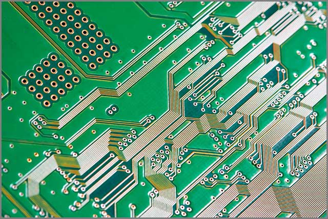
Acid traps are sharp turns and corners in PCB trace patterns that can retain the chemicals used for PCB etching. These chemicals strip away excess copper from a board during the manufacturing process. When collected in an acid trap, the chemicals risk eroding the traces by tunnelling through the mask covering the trail. One of the first rules of thumb any novice PCB designer learns is to avoid acute angles (angles that are less than 90 degrees) in their layout design. Most seasoned designers frown on even the use of right angles. Acid traps are the main leading reason for this rule to come up.
The examples above showed us that using specific design guidelines and avoiding acid traps in your PCB design is essential. In order to understand how acid traps happen, it's helpful to look at the process of manufacturing a Printed Circuit Board.
During step 4 when we use chemical etchants to remove excess copper from the board's surface the acid trap problem will arise. When acid traps are present in the trace layout, they can act as catchments for these corrosive chemicals and harm the copper trace. Let's take a look at some familiar sources of acid traps.
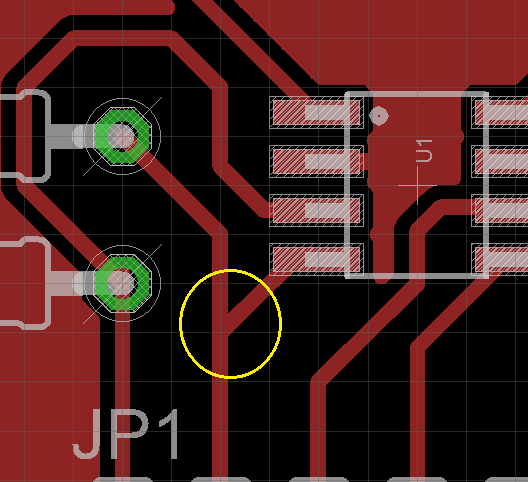
The primary source of acid traps are traces that join at angles under or at 90 degrees. While you can avoid using sharp turns in your designs after acquiring moderate experience, even experience designers can miss the sharp corners that form when joining two traces together. The below image shows such a design, with the problematic joint circled in yellow. The area you mentioned will make the etching solution pooled there. This will lead to the erosion of the copper traces and might cause an open circuit.
Just because you can design components that are contained within a really small space doesn't mean it's a good idea. While it is maybe beneficial from a power integrity standpoint, any tight space can act as an acid trap, and a short circuit can be resulted causing disastrous results. Therefore, it's ideal to leave a bit of tolerance when deciding the gaps between pads, traces, vias, etc., to account for manufacturing errors and also to avoid acid traps. Keeping minimum gaps in most PCB design software saves you a lot of time.
These are copper areas without any actual use. Not only do these copper islands act as acid traps, but they can also cause signal interference issues. Back in the day, when PCB manufacturing was a rather expensive process, designers would leave portions of unused copper without etching in order to reduce the number of etchants used. Nowadays, it's best to remove these dead copper areas and later save yourself from a headache.
PCB designing and routing used to be a rather tedious process in the past, but now a large portion of the workflow can be automated in software that introduces new features with each version. However, when these systems' design rules aren't properly calibrated, they can produce layouts with acid traps. It is within best practices to check your PCBs manually after going through any design automation process.
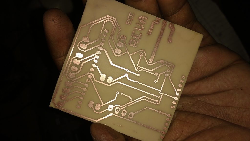
Traditionally, corrosive chemical solutions are used to dissolve the excess copper layer.
If your plans to create a PCB include any of these etching materials, paying attention to your layout and avoiding acid traps is a good idea.
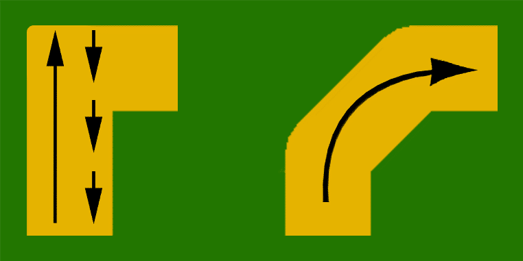
As we discussed above, 90 degrees or fewer angles are acid traps' main sources. As shown in the figure below, we can modify the right angles in our designs to include two 45-degree angles. Not only will this help you avoid acid traps, but if your design contains digital logic or high-speed communication, sticking to 45-degree angles will help you avoid signal reflections that cause interference.
The photosensitive approach to PCB Manufacturing includes using chemicals that are activated underneath UV light. They don't react much unless they are exposed to the proper kind of lighting. The lack of light prevents the etchant from doing too much harm if it is in a section of the board that is blocked off. Copper layers that are even thicker work well with photoactivated etchants. They provide cleaner edges, which can assist in lessening acid buildup in some regions. These etchants also tend to be less corrosive, so they won't harm the copper layer as much as conventional chemicals, even if they get stuck in any corners. Due to its propensity to produce better results, this strategy is currently the most popular.
If you notice a spot that could turn into an acid trap, you might want to add a via or two. By allowing the acid to flow to the opposite side of the board, we can protect traces and other components on the signal layer from acid traps. You must proceed cautiously to avoid drilling through anything significant on either side. This method works well for single-sided boards and shouldn't be used with multi-layered boards.
However, using multiple vias can be a risk of its own. Multiple vias placed close together can form pockets that act as an acid trap. Make sure your design maintains gaps between vias to separate them from each other and copper traces.
The process of streamlining an engineering process for creating an electrical device is known as Design for Manufacturing (DFM). When prototype circuit boards are being developed, more attention is paid to the board's functionality instead of the board's ability to be manufactured. DFM tests ensure that the selected manufacturer can manufacture the PCB by checking the manufacturer's specified parameters.
Most modern PCB designing software comes with DRC functionalities that let you define design rules such as minimum gaps between traces, trace widths, etc. The DRC then checks your PCB layout against these rules to determine whether your design meets the specified requirements. You can check the angles using this. Remove dead copper from your design. Remove any small gaps that can act as acid traps. Running DRC is a mandatory step if your design contains multiple signal or ground layers.
No matter how good you are, errors can still be present in your design from time to time. Even DRC isn't perfect; you can't always depend on it to spot your mistakes. Before sending your design to the manufacturer, carefully review it to see if it follows all the guidelines we've listed. If you're working with a team, the second set of eyes looking at the design might be able to catch any issues that have slipped by you. There are many Gerber viewers that you can use. They can help you see if your layers line up and spot any possible problems before you send your design to the manufacturer.
While most PCB designers from a few decades ago have religiously followed these design rules to avoid acid traps, you might've noticed that many modern PCB designs contain right angles, acute angles, and PCBs with relatively small form factors that have tiny gaps between pads. The majority of PCB manufacturers vastly improving their facilities and fine-tuning their capabilities causes this change in mindset.
Furthermore, the fabrication facilities of today are better equipped and have stricter controls. Manufacturers can still remove extra etching solution, even when the photoresist isn't used.
So as long as you pay attention to your manufacturer's capabilities and choose a manufacturing facility that uses these methods, acid traps won't trouble you or your designs. You can get the parameters for the design rules from the manufacturer's website when creating the design, so you'll make a PCB that they can easily manufacture. But of course, if you're a hobbyist etching your PCB with Ferric Chloride, stick to guidelines and the adages to prevent acid traps from ruining your designs. By following the correct steps in the procedure, you can overcome this problem.
Still, need help? Contact Us: support@nextpcb.com
Need a PCB or PCBA quote? Quote now


 Surface

