
 NextPCB Capabilities
Printed Circuit Boards
NextPCB Capabilities
Printed Circuit Boards
 PCB Assembly
 Layer Buildup
 SMD-Stencils
 PCB Design-Aid & Layout
 Mechanics
 Quality
 Drills & Throughplating
 Factory & Certificate
 PCB Assembly Factory Show
Certificate
PCB Assembly Factory Show
Certificate

Support Team
Feedback:
support@nextpcb.com


A PCB can have one layer, two layers, or dozens of layers. For many commercial designs, 1–32 layers is a practical range, although the exact limit depends on the pcb manufacturer, materials, board thickness, and via structure. At the extreme end, specialist manufacturing has demonstrated boards with 124 layers—but that is a highly specialized capability, not a typical production option. The right layer count is not the highest one a manufacturer can build. It is the lowest count that meets your routing, signal-integrity, power-distribution, size, reliability, and cost requirements.
In everyday PCB manufacturing, boards commonly range from 1 to about 30 or 32 layers, depending on the fabricator. Some specialist manufacturers support more. In a published technical paper, OKI described developing a 124-layer PCB for semiconductor test equipment. That example shows what advanced, application-specific manufacturing can achieve—not what most PCB suppliers routinely offer.
| Category | Typical Layers | Representative Applications |
|---|---|---|
| Single/Double-sided | 1–2 | Simple controllers, LED lighting, toys |
| Standard multilayer | 4–8 | Smartphones, PC motherboards, IoT devices |
| High-density multilayer | 10–20 | High-performance servers, medical imaging |
| Ultra-high layer count | 30+ | Aerospace, supercomputers, ATE, AI accelerators |
A critical nuance: layer count alone doesn't tell the full story. A 20-layer HDI board with sequential build-up is a fundamentally different manufacturing challenge than a 20-layer through-hole board. The stackup architecture matters as much as the number.
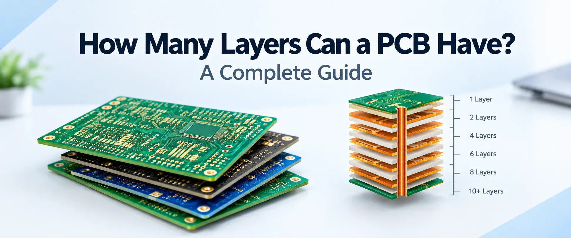
A simple low-speed controller may fit on one or two copper layers. A dense design may need many more. The decision usually comes down to the interaction of routing, electrical performance, physical constraints, and manufacturability.
Circuit Complexity and Component Pitch
As electronic components become smaller and feature higher pin counts (such as fine-pitch BGAs), routing trace paths on a single plane becomes physically impossible. Adding layers provides the necessary vertical real estate to route complex interconnections without signal crossovers.
Signal Integrity (SI) and Electromagnetic Compatibility (EMC)
Every high-speed signal trace (above 50 MHz) needs a continuous reference plane adjacent to it. This single rule — "every signal layer gets a reference plane" — effectively doubles your required layer count. For designs running PCIe Gen 5/6, DDR5, or 100G/400G Ethernet, you're not just adding signal layers; you're adding ground and power planes to maintain impedance control and suppress EMI.
Space and Form Factor Constraints
Modern electronics demand maximum functionality in minimal space. Smartwatches, earplugs, and compact medical sensors cannot expand horizontally. Increasing the Z-axis (adding layers) allows engineers to shrink the overall PCB footprint.
Power delivery and thermal requirements
Boards with many power rails, high-current circuits, or demanding noise constraints may need more carefully allocated copper for power distribution and heat management. Copper distribution, plane continuity, component placement, and material selection all matter. Adding layers alone does not solve thermal or power-integrity problems.
There's a reason most fabs stop at 30 layers. Beyond that threshold, every manufacturing step becomes exponentially more difficult.
This is where engineering judgment matters most. The goal isn't to minimize layers at all costs — it's to find the sweet spot between performance, reliability, and manufacturability. Use this sequence before committing to a layer count:
Start with signal speeds. If your design runs at low speed or DC only, 1–2 layers will do. Once you introduce controlled-impedance signals, you need at least a 4-layer stackup with a solid ground plane. TI's application notes recommend at least 6 layers for boards with multiple high-speed signals, precisely because each signal layer needs a clean reference plane.
Count your power domains. Each distinct voltage rail requiring tight regulation typically needs its own plane or large pour. A design with three or more power rails will almost certainly push you past 6 layers.
Respect the "reference plane per signal layer" rule. This is non-negotiable above 50 MHz. If you're trying to route high-speed signals between two signal layers with no adjacent ground plane, you're building EMI problems into the board that no amount of shielding can fully fix.
Calculate the cost-benefit honestly. In many cases, going from 4 to 6 layers adds 30–40% to board cost but dramatically simplifies routing and improves signal integrity. Conversely, if you can meet EMC requirements at 6 layers instead of 8, you save significant money without sacrificing performance.
Talk to your fabricator before you finalize the stackup. Manufacturer capabilities — minimum drill diameter, line width/spacing, maximum lamination layers, and available prepreg thicknesses — vary widely. Catching a stackup issue before layout saves 2–4 weeks compared to discovering it at DFM review. Get their actual material Dk values and prepreg data, not catalog specs.
A practical rule of thumb: choose the minimum layer count that allows every high-speed signal to have a continuous reference plane, every power domain to have adequate copper, and every fine-pitch component to escape cleanly. Then add one pair of layers as margin if your routing density exceeds 70% of available channels.
So, how many layers can a PCB have? While standard commercial production routinely handles 1 to 32 layers, advanced manufacturing techniques allow for 100+ layers in ultra-complex systems.
For the vast majority of commercial projects, staying within 4 to 16 layers yields the best balance between technical performance, manufacturing reliability, and cost-efficiency.
> Recommend reading: A Step-by-Step Guide to PCB Fabrication Process
Is there a maximum number of PCB layers?
There is no single universal maximum. The limit depends on the manufacturer's equipment, materials, board dimensions, and process.
Does a higher layer count always improve PCB performance?
No. More layers can provide routing space and allow more deliberate separation of signals and planes, but performance also depends on stackup design, return paths, impedance, materials, vias, and layout.
How many layers does a high-speed PCB need?
There is no universal number. Start with the interface and design constraints, then plan a stackup that provides suitable reference planes and routing. Consult the component manufacturer's layout guidance and your PCB fabricator before finalizing the count.
Need Help Optimizing Your PCB Stackup? Choosing the right layer count early saves cost and prevents costly redesigns. Contact our engineering team today or submit your Gerber files for a free DFM review and stackup analysis.
Still, need help? Contact Us: support@nextpcb.com
Need a PCB or PCBA quote? Quote now




