
 NextPCB Capabilities
Printed Circuit Boards
NextPCB Capabilities
Printed Circuit Boards
 PCB Assembly
 Layer Buildup
 SMD-Stencils
 PCB Design-Aid & Layout
 Mechanics
 Quality
 Drills & Throughplating
 Factory & Certificate
 PCB Assembly Factory Show
Certificate
PCB Assembly Factory Show
Certificate
Support Team
Feedback:
support@nextpcb.com


Technological advancements have led to smaller, lighter electronics. Surface-mount technology (SMT) was developed in response to consumer demands. However, this increased demand demanded fast-assembling high-density technologies for these products. BGAs were created because of this push. PCB chip designs have quickly adopted BGAs and other similar devices. However, the difficulty in inspecting these devices after assembly is well known.
This article discusses the BGA chips, soldering processes, and challenges associated with BGA inspection.
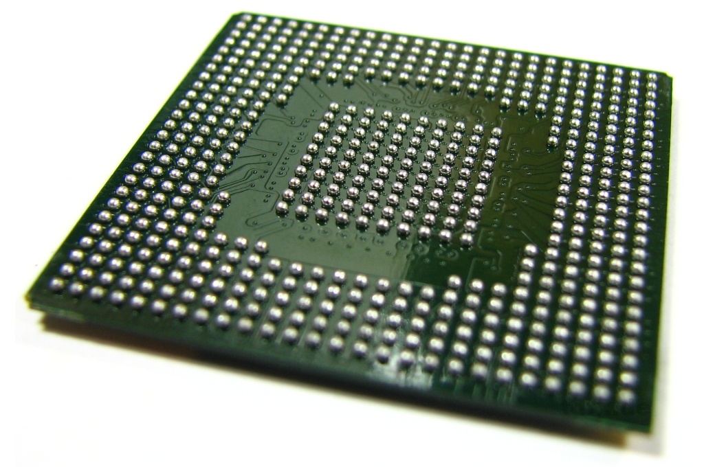
Ball Grid Array (BGA) is a type of surface-mount packaging technology used for integrated circuits (ICs) in electronic devices. BGA chips consist of an IC mounted on a substrate, with an array of solder balls on the underside that provides electrical connections to a printed circuit board (PCB). The solder balls are arranged in a grid pattern, giving the package its name.
BGA chips use solder balls to pass the electricity between the circuit board and the boxes. These balls use wire bonding to make the electrical connection with the die. The substrate consists of a conductive trace that sends the electric signal from bonds between the substrate between the balls and the base.
The significant advantage of a BGA chip is it reuses the components that save the material's cost by reconnecting the BGA chips.
The BGA chips are designed to take up less space on the circuit board than their counterparts, making them an ideal option for electronics that need to be compact. This space-saving design allows for higher density and complexity of circuits.
The ball shape of the BGA chip's joints aligns with the package, ensuring a more precise and accurate alignment of the chip on the circuit board. This self-alignment characteristic reduces the risk of errors and misalignment during the manufacturing process, making the BGA chip more reliable.
The BGA chip's small size and the high number of joints make it more conductive than other chip types. The higher conductivity reduces the risk of signal interference and makes it an ideal option for high-speed and high-frequency circuits.
BGA chips are designed to dissipate heat more effectively than their counterparts. The design of the BGA chip allows for more efficient heat transfer, ensuring that the chip stays cool and runs efficiently.
BGA chips come with larger solder pads, making it easier to rework and desolder them. This feature ensures that the chips can be repaired and replaced with ease, reducing the downtime and cost of repairs.
The design of the BGA chip allows for higher yields during the manufacturing process, reducing the cost of production. This, combined with the ease of rework and desoldering, makes the BGA chip a more cost-effective option compared to other chip types.
BGA chips are known for their high lead count, which allows for more electrical connections to be made between the chip and the PCB. Unlike traditional packaging methods like Quad Flat Package (QFP) or Dual In-line Package (DIP), BGA chips use an array of solder balls on the bottom of the package to create electrical connections. This arrangement allows for a higher number of connections within a smaller area, enabling the integration of more complex and powerful chips in electronic devices.
Inductance is an electrical property that can cause signal degradation, especially in high-frequency applications. BGA chips have a lower inductance compared to other packaging types because of their shorter electrical paths between the chip and the PCB. This reduced inductance helps to minimize signal distortion and improve the overall performance of the electronic device, making BGA chips an ideal choice for high-speed applications.
BGA chips offer high interconnection density due to their unique packaging design. The solder balls in the BGA package are arranged in a grid pattern, which allows for more connections per unit area compared to other packaging methods. This high interconnection density enables the integration of more features and functions in a smaller form factor, leading to the development of compact and high-performance electronic devices.
One of the main advantages of BGA chips is their small footprint on the PCB. Since the electrical connections are made through solder balls on the bottom of the package, there are no protruding leads that require additional space. This compact design allows for more efficient use of the board area and facilitates the development of smaller and thinner electronic devices.
Unlike other packaging types that have exposed leads, BGA chips have no leads that could bend or break. This feature improves the overall mechanical reliability of the chip package and reduces the chances of damage during assembly, handling, or operation. Furthermore, BGA chips are less prone to issues like lead fatigue or solder joint cracking, which can occur in packages with protruding leads.
BGA chips exhibit low thermal resistance between the chip package and the PCB. The solder balls in the BGA package provide a direct thermal path from the chip to the PCB, allowing for efficient heat dissipation. This efficient heat transfer helps to maintain the chip's optimal operating temperature, resulting in improved performance and increased reliability. Additionally, BGA chips can be paired with additional heat dissipation solutions, such as heat sinks or thermal vias, to further enhance their thermal management capabilities.
The common BGA PCB chip types include:
CBGA, a ceramic ball grid array package, uses a ceramic substrate. The CCGA and LGA packages fall under this category. Each pin of CBGA costs more compared to other package types. The application that takes the high pin count on flip flops requires this CBGA.
Thus, in general, ceramic BGA packages work well with flip chips. In order to increase reliability and overcome thermal expansion differences between the substrate and board, the solder balls contain 90 percent lead and 10 percent tin. This makes the BGA more reliable and trustworthy. The life span of the solder joints increases 3 times with the CGA package type compared to the BGA.
The plastic ball grid array package uses solder balls and a plastic substrate. This combines 63% of tin and 37% of eutectic lead. This substrate is capable of bearing a temperature of 150 degrees. The selection of this material includes:
It also supports the flip-flop design, providing better connectivity between the package and the circuit board.
Tape BGA creates fine lines on the solder balls by using the flexible interconnect. It provides a thicker version of BGA, providing better thermal and electrical performance. In the simplest design form, this package uses an aluminum substrate. It also makes use of the thin film and the microchip module that connect the solder mask to the aluminum base.
This package allows the heat sink and chip to face down. The downward facing of the chip should use flip-chip technology. At the same time, the wire bond is used if your chip faces up. This is excellent for an application that requires high-efficiency and thin packages. This makes the higher cost of the PBGA.
Another form of PBGA, TEBGA (Thermal Enhanced Ball Grid Array), differs in only one aspect, which is the addition of heat sinks. Heat sinks are directly attached to chips with their faces down, and electrical connections are made by wire bonding. It uses a liquid compound to seal the chip after building a dam around it.
PoP is the package on the package that is of double stack design. Among the two chips, the uppermost chip is the RAM, while the lower chip is the CPU. This package design allows more packages to get fit into a smaller footprint on the circuit board.
The land grid array package uses the solder balls for the effective connection of the circuit board and the package.
QFN, a quad flat no-lead pack. This design is a variation of the QFP packages with no pins. The quad-flat package sends the leads from all four sides and is a surface-mounted chip.
Flip Chip BGA makes use of the BT resin in place of the Ceramic as a substrate material. For flip chips, these BGAs are soldered with tin and lead in a ratio of 63:37, as a result of which they self-align without the use of expensive and accurate alignment machines. This BGA chip improves electrical performance and saves cost, and reduces the internal circuit loops. One of the additional advantages of using this Flip-Chip is the distance shrink and reduced inductance.
Place the BGA PCB chip on the PCBA pads after applying dense flux to the BGA tin balls. It is important to glue the BGA and position it so that it will not be blown away by the wind. In any case, it is important not to put in too much flux.
When heating, the excessive bubbles of rosin can be shifted. Additionally, the PCBA board must be placed level on the BGA rework platform, with the appropriate nozzle changed, left 4 mm from the chip, the primary temperature curve set to the BGA rework station, and the automatic soldering screen clicked.
As the BGA tin ball melts, the PCBA solder pads are formed, and the surface tension of the tin ball causes the chip to center even if it is separated from the motherboard. BGA soldering will be completed when the BGA repair table is heated. When the BGA repair table is heated, however, an alarm will sound.
Yes, BGA chips do need the solder paste applied in the PCB pads before the assembly process. Solder paste is the mixture of solder balls and the flux, while BGA solder paste is the type of solder having a lower diameter and various melting temperatures. It is applied to the surface mount pads on the PCB with the use of the stencil.
When the BGA PCB chip is assembled, it is placed on top of a paste of solder balls, then heated to melt them. A secure and reliable connection is then formed between the BGA PCB chip and the PCB pads with the help of melted solder.
Generally, the BGA chip contains pads that are not connected or are connected to other pads in the board. Thus, the BGA chip requires soldering to complete the circuit.
Inspecting the BGA chip is the prior thing to consider before shipping them to the market. BGA inspecting is the quality control method that ensures the solder joint's quality. It can troubleshoot various defects, including cold solder joints, solder ball defects, and bridging and voiding defects.
Some of the key parameters to consider while inspecting the BGA chip includes the following:
Thus, the manufacturer uses various tools and techniques for BGA chip inspection and finds the parameters and features of the chip.
Some of these tools and techniques used in inspecting the BGA chip include
This technique involves applying electrical signals to the BGA chip and measuring the response. The response includes the electrical stability of the board. Electrical testing can detect defects such as short circuits, open circuits, and incorrect pinouts.
X-rays inspect the BGA solder joints. It helps to inspect and check through the device's solder joints beneath the components. Besides, there is another inspection test available that includes a manual test, an AOI test, and functional testing.
This technique uses a microscope or specialized camera to inspect the external surface of the BGA chip and the surrounding PCB. Optical inspection can detect defects such as misalignment, insufficient solder paste, and solder ball defects. The major benefit of this visual inspection is that it is easier to carry and doesn't require any expensive devices. One of the famous visual inspection techniques includes the endoscope.
An endoscope enables technicians to visually inspect connections between a BGA and PCB. With good lighting, we can also observe some interior rows as well. A solder joint can be assessed based on its shape, surface texture, appearance, and quality using this optical technique.
While BGA chips offer several advantages, they can also be susceptible to various defects during manufacturing, assembly, and operation, such as misalignment, missing balls, voiding, inconsistent standoff height, not-wetted pads, open circuits, popcorning, and bridges. Understanding and addressing common BGA defects is crucial for ensuring the reliability and performance of electronic devices. By implementing proper manufacturing, assembly, and handling practices, these defects can be minimized or eliminated, resulting in better-quality BGA chips and more reliable electronic products.
Misalignment occurs when the BGA package is not accurately aligned with the corresponding pads on the PCB during assembly. This can result in poor electrical connections, reduced performance, or even device failure. Misalignment can be caused by factors such as inaccurate placement equipment, warping of the PCB or BGA package, or inconsistencies in solder ball size.
Missing balls refer to the absence of one or more solder balls on the BGA package. This can lead to open circuits, resulting in device malfunction or failure. Causes of missing balls can include manufacturing defects, damage during handling, or improper reflow soldering process.
Voiding refers to the presence of air pockets or voids within the solder joints, which can compromise the mechanical and electrical integrity of the connection. Voids can occur due to trapped gases during the reflow soldering process or contamination of solder paste. Excessive voiding can lead to increased thermal resistance, reduced electrical conductivity, and potential device failure.
Standoff height refers to the distance between the BGA package and the PCB. Inconsistent standoff height can lead to uneven stress distribution on solder joints, increasing the likelihood of joint failure. Causes of inconsistent standoff height include variations in solder ball size, warping of the PCB or BGA package, or uneven solder paste application.
Not-wetted pads occur when the solder does not adequately wet the pad on the PCB or the BGA package, resulting in weak or incomplete solder joints. This can lead to open circuits or intermittent electrical connections. Not-wetted pads can be caused by factors such as contaminated or insufficient solder paste, oxidation on pad surfaces, or improper reflow soldering profile.
Open circuits refer to breaks in the electrical connection between the BGA package and the PCB. Open circuits can be caused by various factors, including missing balls, not-wetted pads, or poor solder joint quality. Open circuits can result in device malfunction or complete failure.
Popcorning is a phenomenon in which moisture absorbed by the BGA package expands during the reflow soldering process, causing the package to crack or delaminate. This can lead to mechanical and electrical failures in the device. To minimize the risk of popcorning, proper storage and handling practices should be followed to limit moisture exposure.
Bridging occurs when solder balls on the BGA package inadvertently connect adjacent pads on the PCB, creating an unintended electrical connection. Bridging can result in short circuits, leading to device malfunction or failure. Causes of bridging include excessive solder paste application, misaligned BGA packages, or improper reflow soldering profile.
NextPCB is one of the leading PCB suppliers in China. We help our customers to achieve quality products without compromising the cost. Please feel free to ask anything about BGA quality control and inspection through our contact details.
Still, need help? Contact Us: support@nextpcb.com
Need a PCB or PCBA quote? Quote now


 Surface

