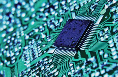
Powering the Communication Industry
The communication industry forms the backbone of global connectivity. From telecom infrastructure and wireless networks to high-speed data transmission systems, reliable electronic hardware is essential to ensure stable, low-latency communication. As technologies such as 5G, cloud computing, and IoT continue to evolve, the performance requirements placed on PCBs used in communication equipment have increased significantly. NextPCB supports communication industry customers with PCB manufacturing and assembly solutions designed to meet these growing technical and reliability demands. >>> Get an Advanced PCB Quote
Industry Challenges in Communication Electronics
Electronic systems used in the communication industry face several common challenges:
- Increasing operating frequencies and data rates
- Strict signal integrity and impedance requirements
- Heat generation from RF and power components
- Complex multilayer designs for dense routing
These challenges make PCB design and manufacturing a critical factor in the success of communication products.
How PCBs Enable Communication Systems
PCBs used in the communication industry serve as the foundation for signal transmission and power distribution.
To ensure stable performance, communication PCBs often require:
- Low-loss materials for high-frequency signals
- Controlled impedance for high-speed data paths
- Advanced thermal management solutions
- Precise manufacturing for multilayer structures
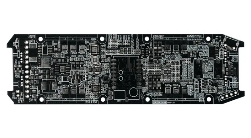
How NextPCB Supports the Communication Industry
NextPCB provides end-to-end PCB solutions tailored to the needs of communication equipment manufacturers:
- Material Expertise: Support for standard FR4, high-speed laminates, and high-frequency materials such as Rogers and Isola
- Advanced Manufacturing: Backdrilling, hybrid stack-ups, resin plugged vias, and impedance-controlled fabrication
- Engineering Support: DFM review focused on signal integrity and manufacturability
- Assembly & Testing: PCB assembly for RF modules, BGAs, and functional testing
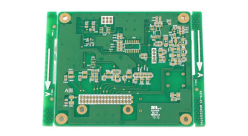
Typical Communication Industry Applications
Our PCB solutions are widely used in:
- Telecom infrastructure equipment
- 4G / 5G base stations and small cells
- Networking and data communication hardware
- RF modules and wireless communication devices
- Satellite and microwave communication systems
Need high-frequency, impedance-controlled PCBs for communication equipment?
Communication Industry PCB Capabilities
| Capability |
NextPCB Support |
| Layer Count |
Up to 32 layers |
| Impedance Control |
±10% standard, ±5% high precision |
| Material Options |
FR4, High-Speed FR4, Rogers |
| Surface Finish |
ENIG, Immersion Silver, ENEPIG |
| Special Processes |
Backdrilling, Hybrid Lamination |
PCB Capabilities Supporting This Industry
Advanced PCB Manufacturing Capabilities
Multi-layer, fine-line, and high-reliability PCB processes for demanding industrial applications.
Learn More
High-Frequency & Advanced PCB Materials
Rogers, PTFE, and specialty laminates engineered for stable electrical performance.
View Materials
Frequently Asked Questions
What types of PCBs are commonly used in the communication industry?
Multilayer PCBs with controlled impedance and low-loss materials are commonly used in telecom and wireless communication equipment.
Can NextPCB support both prototyping and volume production?
Yes. We support rapid prototyping as well as stable mass production for communication industry customers.
Do you offer PCB assembly for communication products?
Yes. NextPCB provides PCB assembly services for communication devices, including RF modules and high-density designs.
Partner with NextPCB for Communication Industry PCBs
With extensive experience serving the communication industry, NextPCB helps customers bring reliable and high-performance communication products to market. >>> Upload Your Design & Get a Quote
Related PCB Application Industries

 NextPCB Capabilities
 PCB Assembly
 Layer Buildup
 SMD-Stencils
 PCB Design-Aid & Layout
 Mechanics
 Quality
 Drills & Throughplating
 Factory & Certificate
 PCB Assembly Factory Show
Certificate
PCB Assembly Factory Show
Certificate
 NextPCB Capabilities
 PCB Assembly
 Layer Buildup
 SMD-Stencils
 PCB Design-Aid & Layout
 Mechanics
 Surface
 Quality
 Drills & Throughplating
 Factory & Certificate